Surface treatment method of printed circuit board and application of surface treatment method

A printed circuit board, surface treatment technology, applied in the direction of printed circuit, printed circuit manufacturing, electrical components, etc., can solve the problems of ink loss and residual glue, seepage, difficult to meet product requirements, etc., to achieve easy film fading, adhesion Tight, little pollution effect

Pending Publication Date: 2021-10-22
广东世运电路科技股份有限公司
View PDF3 Cites 4 Cited by
  • Summary
  • Abstract
  • Description
  • Claims
  • Application Information

AI Technical Summary

Problems solved by technology

[0003] At present, in the process of circuit board production, the surface treatment methods of partial electroplating thick nickel gold and chemical precipitation nickel gold mainly use heat-cured chemical-resistant gold wet film and expensive selective dry film for surface protection. This method is not only difficult to achieve high precision Requirements, and cannot withstand the high temperature conditions of the chemical nickel-gold process (above 80 ° C), there are quality risks such as penetration, ink loss and residual glue
Moreover, for complex line

Method used


Image

  • Surface treatment method of printed circuit board and application of surface treatment method
  • Surface treatment method of printed circuit board and application of surface treatment method
  • Surface treatment method of printed circuit board and application of surface treatment method

Examples


Embodiment 1

[0062] A method for making a PCB, the specific process is:

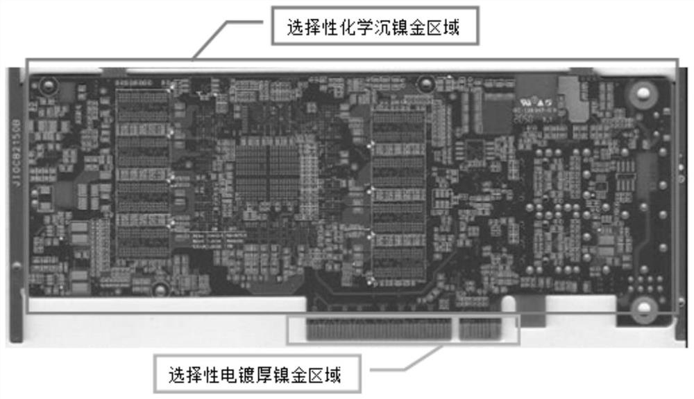
[0063] Pre-process→solder resist→characters→wet film selection→anti-electric gold tape→laser cutting→nickel gold electroplating→film removal→etching→electric gold tape tearing→wet film selection→chemical nickel gold→film removal→after process .

[0064] Specifically, after the pre-production process (pre-process) such as material cutting, inner layer dry film, browning, lamination, drilling, copper plate plating, outer layer dry film, outer layer graphic plating, etc. (it can also be used) character making), and obtain the PCB with the outer layer circuit and the solder resist layer made. After the pre-processing process, the outer circuit in the PCB includes the gold finger area for selective electroplating of thick nickel gold, and the leads drawn from the gold finger area to the edge of the printed circuit board are used for selective electroless nickel gold plating. The chemical immersion gold area, and the rem...


PUM

PropertyMeasurementUnit
Adhesionaaaaaaaaaa
Adhesionaaaaaaaaaa

Abstract

The invention discloses a surface treatment method of a printed circuit board and application of the surface treatment method. When the gold finger area is electroplated with thick nickel gold, the chemical gold immersion area which does not need to be electroplated is protected by adopting an anti-gold-electroplating adhesive tape with the tensile strength of 1.4-1.8 kg/10mm, the elongation of 120%-180% and the adhesive force of 0.08-0.12 kg/25mm. The anti-gold-plating adhesive tape is tightly attached in the electroplating process, the problems of diffusion plating and ink falling of a chemical gold immersion area in the electroplating process are avoided, the anti-gold-plating adhesive tape has the characteristic of no degumming after being torn off, and the quality risk of adhesive residues is avoided. Meanwhile, the anti-gold plating adhesive tape is combined with the specific photosensitive ink, so that the surface treatment method can meet the high-precision requirement that the distance between the chemical gold immersion area and the golden finger area is larger than 6 mil, the production process is simplified, and the manufacturing cost is reduced.

Description

technical field [0001] The invention relates to the technical field of printed circuit board production, in particular to a surface treatment method of a printed circuit board and its application. Background technique [0002] With the ever-changing and multi-functional requirements of electronic products, the integration of IC (chip) and BGA (ball array package) in circuit board design is also getting higher and higher, and the pins of IC and BGA are getting denser, which gives SMT (chip and plug-in) placement and circuit board fabrication pose technical challenges. At the same time, in order to cope with technical improvement and functional flexibility and detachability, different areas of the circuit board have different surface treatment requirements. For example, for segmented card gold finger circuit boards such as information transmission and servers, in order to improve the wear resistance, electrical conductivity and oxidation resistance of the gold finger, it is u...

Claims


Application Information

Patent Timeline
IPC IPC(8): H05K3/00H05K3/10H05K3/18
CPCH05K3/00H05K3/10H05K3/188
Inventor 谢富民苏南兵李嘉健
Owner 广东世运电路科技股份有限公司
Why Eureka
Try Eureka