Thin film pressure sensor and preparation method and application thereof
A thin film pressure and sensor technology, applied in the field of sensors, can solve the problems of small range of semiconductor strain gauges, poor thermal stability, serious nonlinearity, etc., and achieve the effect of good piezoresistive effect, good stability and large piezoresistive coefficient
- Summary
- Abstract
- Description
- Claims
- Application Information
AI Technical Summary
Problems solved by technology
Method used
Image
Examples
preparation example Construction
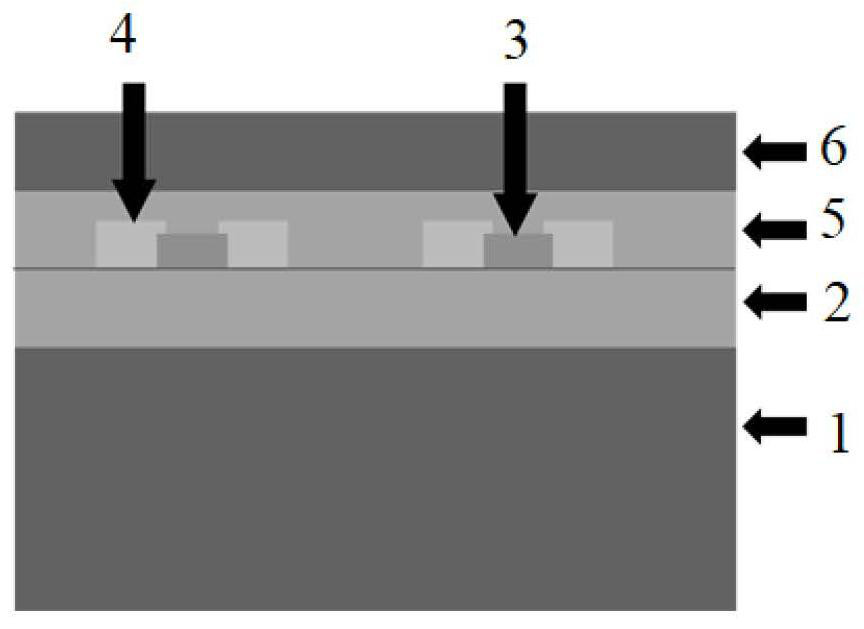
[0066] The present invention also provides a preparation method for the above thin film pressure sensor, comprising the following steps:
[0067] Step 1: depositing the first insulating layer by magnetron sputtering;
[0068] Step 2: Deposit a piezoresistive sensitive layer on the first insulating layer by using a sensitive element mask and magnetron sputtering; the piezoresistive sensitive layer is Cu 84 mn 12 Ni 4 ;
[0069] Step 3: using an electrode mask and magnetron sputtering to deposit an electrode layer on the first insulating layer, and the electrode layer is connected to the piezoresistive sensitive layer;
[0070] Step 4: using magnetron sputtering to deposit a second insulating layer, so that the electrode layer and the piezoresistive sensitive layer are enclosed between the second insulating layer;
[0071] Step 5: Prepare a protective layer on the second insulating layer by arc ion plating.
[0072] In the present invention, the wear-resistant protective la...
Embodiment 1
[0091] This embodiment is the preparation of a thin film pressure sensor, and the specific preparation steps are as follows:
[0092] 1. Substrate pretreatment
[0093] (1) Solvent cleaning treatment: first use deionized water to dissolve the cemented carbide substrate for ultrasonic cleaning for 15 minutes, and then use 95% alcohol for ultrasonic cleaning for 15 minutes.
[0094](2) Glow and ion source bombardment cleaning treatment: use glow to clean the surface of the substrate for 20 minutes, the Ar flow rate is 300 sccm, the cavity pressure is 0.6Pa, and the bias voltage is -600V; then use the Booster ion source to clean the substrate for 10 minutes, The Ar flow rate is 420sccm, the chamber pressure is 0.8Pa, the substrate bias voltage is -200V, and the ion source power is 1200W.
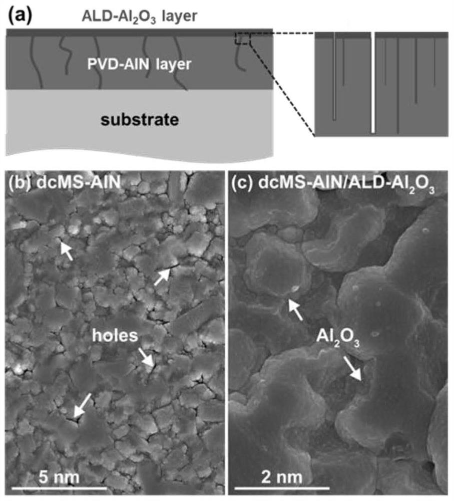
[0095] 2. First deposit the metal AlN insulating layer on the surface of the cemented carbide substrate by magnetron sputtering, and deposit Al by ALD 2 o 3 fill layer
[0096] (1) Al metal...
Embodiment 2
[0114] This embodiment is the preparation of a thin film pressure sensor.
[0115] The difference between this embodiment and embodiment 1 is: deposition of CuMnNi film:
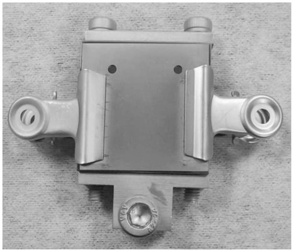
[0116] After the pre-sputtering is completed, the mask plate is fixed and tightly attached to the metal substrate coated with an insulating layer by using a clamp, and then the whole is fixed on the furnace cavity turret of the PVD deposition equipment. Firstly, the cavity temperature is heated and kept at 400°C, the local vacuum is pumped to below 5mPa, Ar is introduced, the flow rate is 300sccm, the bias power is turned on, the bias value is -600V, and the substrate covered with the mask is illuminated. Clean with light for 10 minutes, then reduce the bias voltage to -200V, turn on the power of the Booster ion source, set the power of the ion source to 1200W, and etch the substrate covered with the mask for 2 minutes. Then adjust the Ar flow value to about 240 sccm, maintain the chamber pressure at 0.5 Pa...
PUM
| Property | Measurement | Unit |
|---|---|---|
| thickness | aaaaa | aaaaa |
| thickness | aaaaa | aaaaa |
| thickness | aaaaa | aaaaa |
Abstract
Description
Claims
Application Information


