Micro or nano structure inertia sensor and its production method
A technology of inertial sensor and micro-nano structure, applied in the field of nano-electromechanical system and sensing, can solve the problems of high aspect ratio, unrealizable flexible support, small diameter, etc., to ensure production accuracy, improve sensitivity, and simple production method Effect
- Summary
- Abstract
- Description
- Claims
- Application Information
AI Technical Summary
Problems solved by technology
Method used
Image
Examples
Embodiment 1
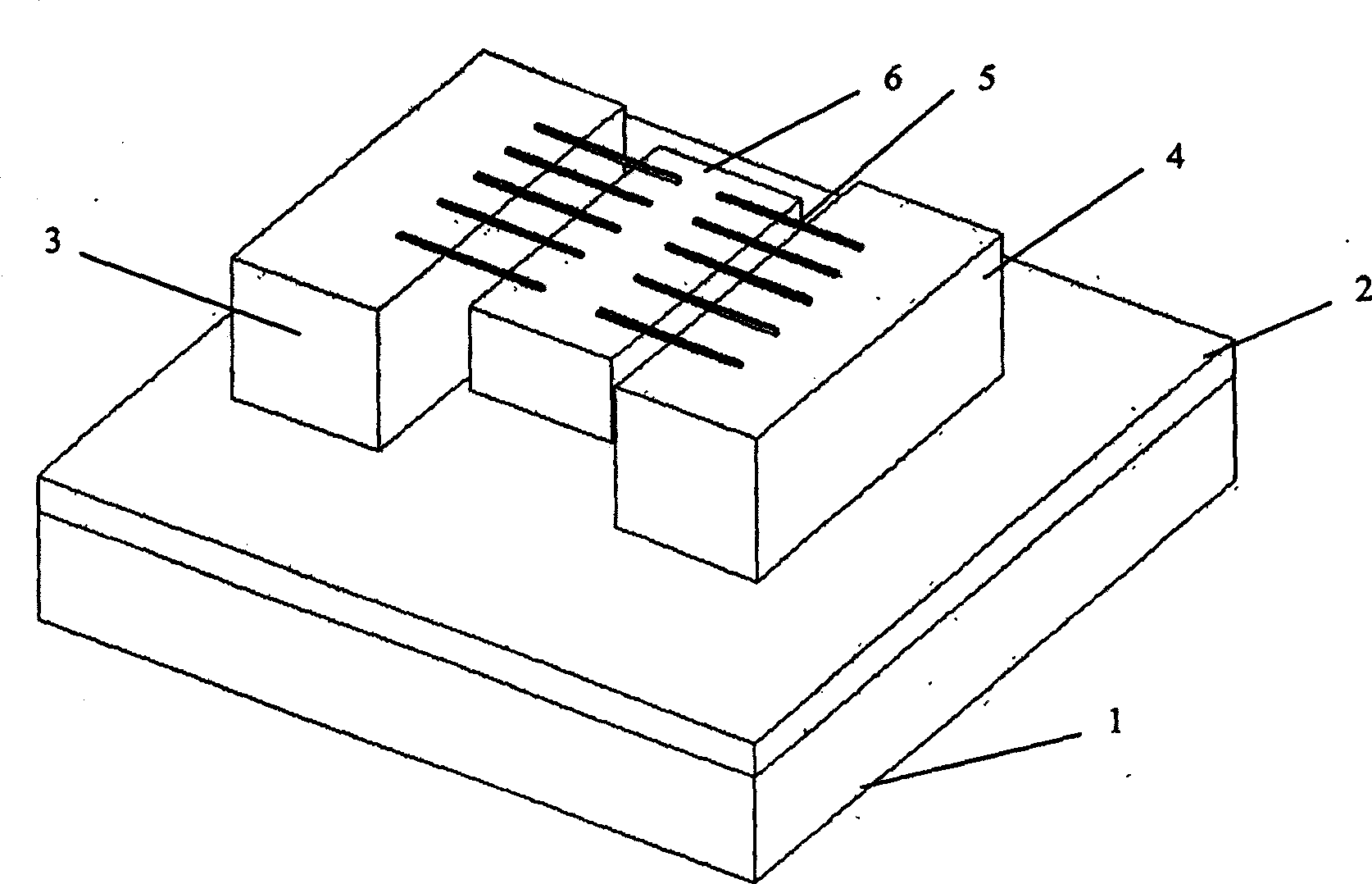
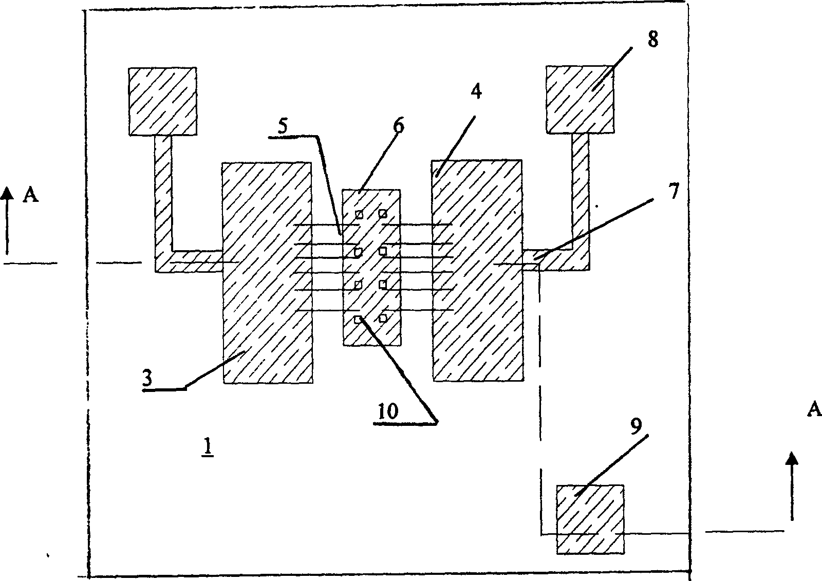
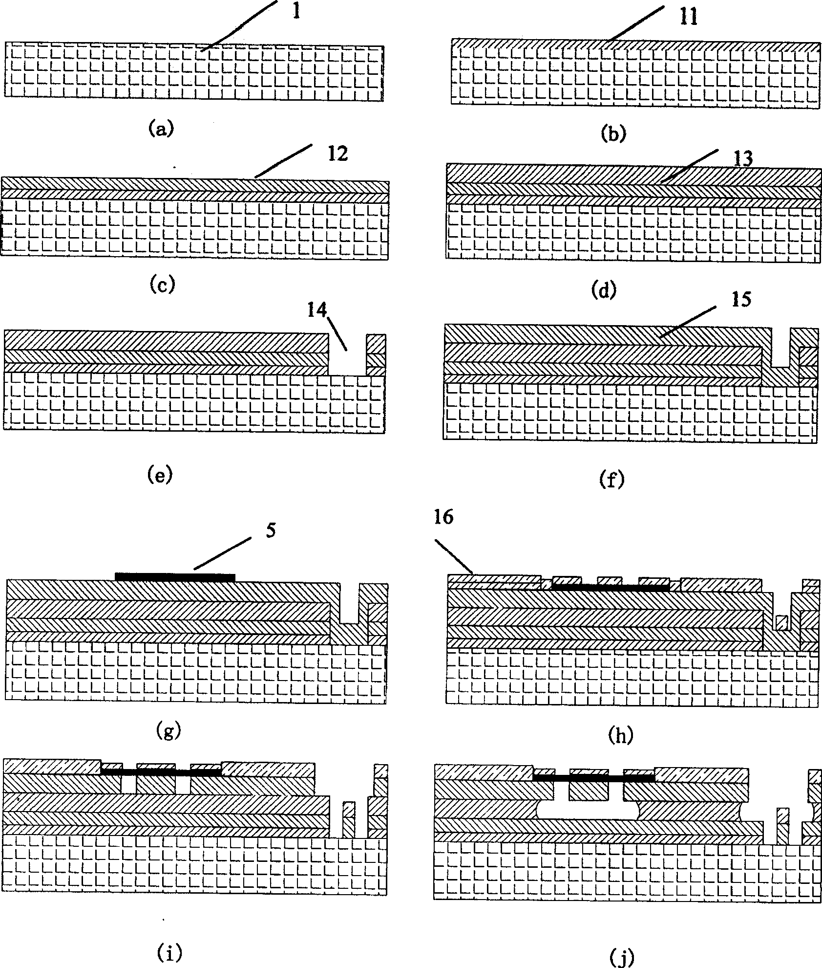
[0038] Embodiment 1, press figure 1 with image 3 As shown, the manufacture of an inertial sensor includes a silicon wafer substrate 1, and the substrate 1 is heavily doped with phosphorus as a driving electrode (bottom electrode). Deposit a layer thickness of 400 on the silicon substrate 1 of silica 11, and 1500 The silicon nitride 12 forms the insulating layer 2, and the first strip-shaped electrode 3 and the second electrode 4 with a length of 100 μm × a height of 2 μm (the width of which is coordinated according to the pattern distribution in the layout) are respectively arranged on the two sides of the insulating layer 2. for polysilicon. A group of 5 resonant beams 5 is overlapped between the first electrode 3 and the mass block 6, and another group of 5 resonant beams 5 is lapped between the second electrode 4 and the mass block 6. At the same time, the carbon nanotubes are also As the electrical leads for the electrical connection between the mass 6 and the elect...
Embodiment 2
[0040] according to figure 1 As shown, the manufacture of an inertial sensor includes a silicon wafer substrate 1, and the substrate 1 is heavily doped with phosphorus as a driving electrode (bottom electrode). A layer thickness of 1000 is deposited on the silicon substrate 1 of silica, and 1500 Silicon nitride forms an insulating layer 2, and on both sides of the insulating layer 2, a first strip-shaped electrode 3 and a second electrode 4 with a length of 100 μm×a height of 2 μm (the width of which is coordinated according to the layout in the layout) are respectively arranged. The electrodes are polysilicon. A group of 10 platinum metal nanowires is used as a resonant beam 5 with a length of 15 μm and a diameter of 20 nanometers. The resonant beam 5 passes through the mass block 6 from the first electrode 3 to the second electrode 4. The nanowires are also used as electrical leads for electrical connection between the mass block 6 and the electrodes 3 and 4 . By corro...
Embodiment 3
[0042] according to figure 1 As shown, the manufacture of an inertial sensor includes a silicon wafer substrate 1, and the substrate 1 is heavily doped with phosphorus as a driving electrode (bottom electrode). Deposit a layer thickness of 500 on the silicon substrate 1 of silica and 1700 The insulating layer 2 is formed of silicon nitride, and the other structures are the same as in the embodiment 1, except that the resonant beam 5 uses GaP semiconductor nanowires, the length of which is between 15 μm and the diameter of 60 nanometers. The mass block 6 is located at the center of the upper part of the insulating layer 2, the mass block is suspended under the support of the resonant beam, and the gap (air gap) between the insulating layer 2 and the mass block 6 is 2.5 μm; and the mass block 6 passes through 2 groups The elastic beam 5 of carbon nanotubes is fixed in the middle of the first electrode 3 and the second electrode 4, and the gap between the mass block 6 and the...
PUM
 Abstract
Description
Claims
Application Information


