

Power on reset circuit capable of generating power on reset signal without fail
A reset circuit and reset signal technology, which is applied in data reset devices, electrical components, electronic switches, etc., can solve the problems that power-on reset signals cannot be generated, internal circuits are not reset, etc.
- Summary
- Abstract
- Description
- Claims
- Application Information
AI Technical Summary
Problems solved by technology
Method used
Image

Examples
Embodiment 1
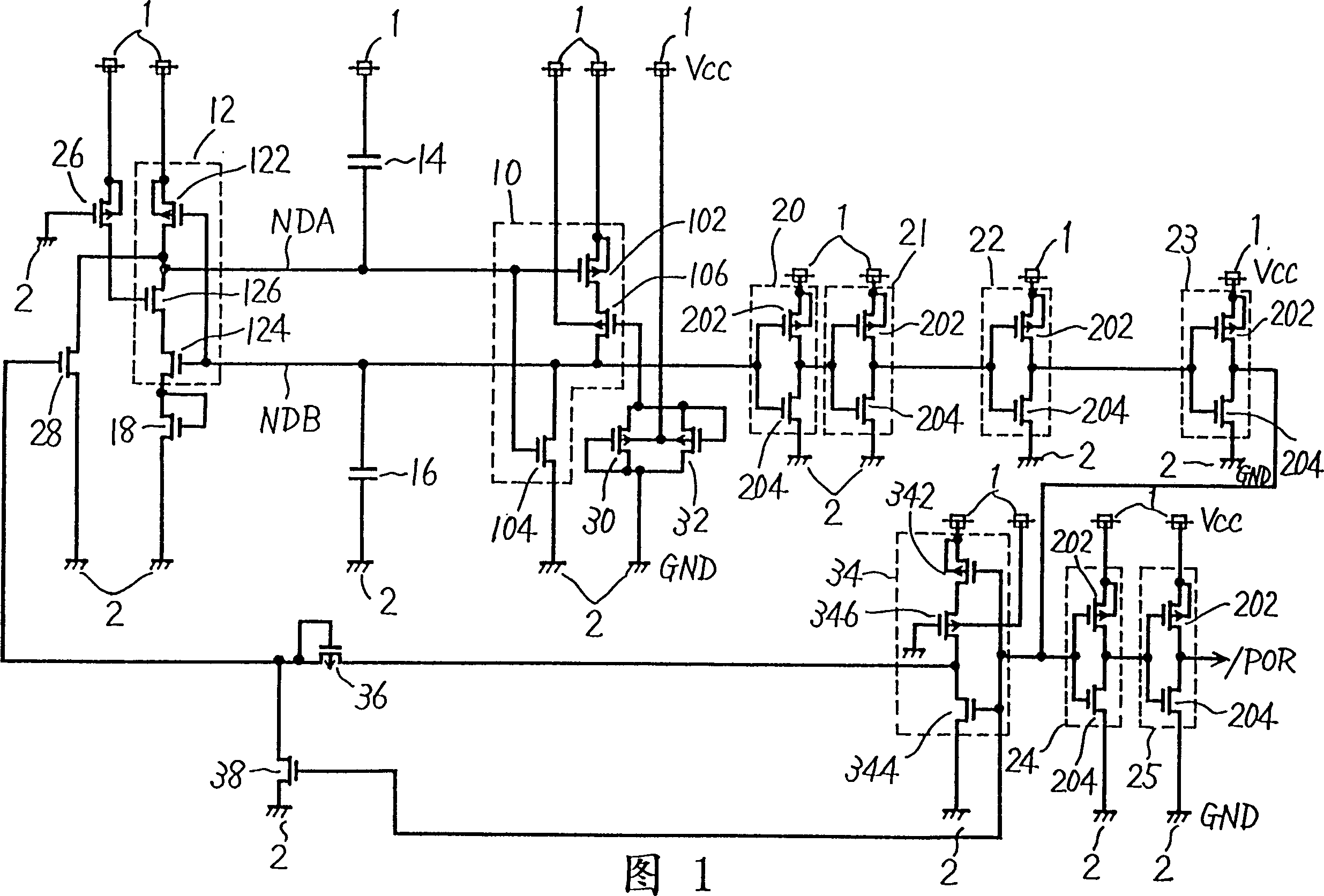
[0020] FIG. 1 is a circuit diagram showing the overall configuration of a power-on reset circuit according to Embodiment 1 of the present invention. Referring to FIG. 1 , the power-on reset circuit includes CMOS inverter circuits 10 and 12 , a capacitor 14 and an N-channel MOS transistor 18 .
[0021] The CMOS inverter circuit 10 includes a P-channel MOS transistor 102 , an N-channel MOS transistor 104 and a P-channel MOS transistor 106 . P-channel MOS transistor 102 has a gate connected to node NDA, a source connected to power supply node 1 , and a drain connected to node NDB through P-channel MOS transistor 106 . N-channel MOS transistor 104 has a gate connected to node NDA, a drain electrically connected to node NDB, and a source connected to ground node 2 . P-channel MOS transistor 106 is connected between P-channel MOS transistor 102 and node NDB.
[0022] The CMOS inverter circuit 12 includes a P-channel MOS transistor 122 , an N-channel MOS transistor 124 and an N-cha...
Embodiment 2
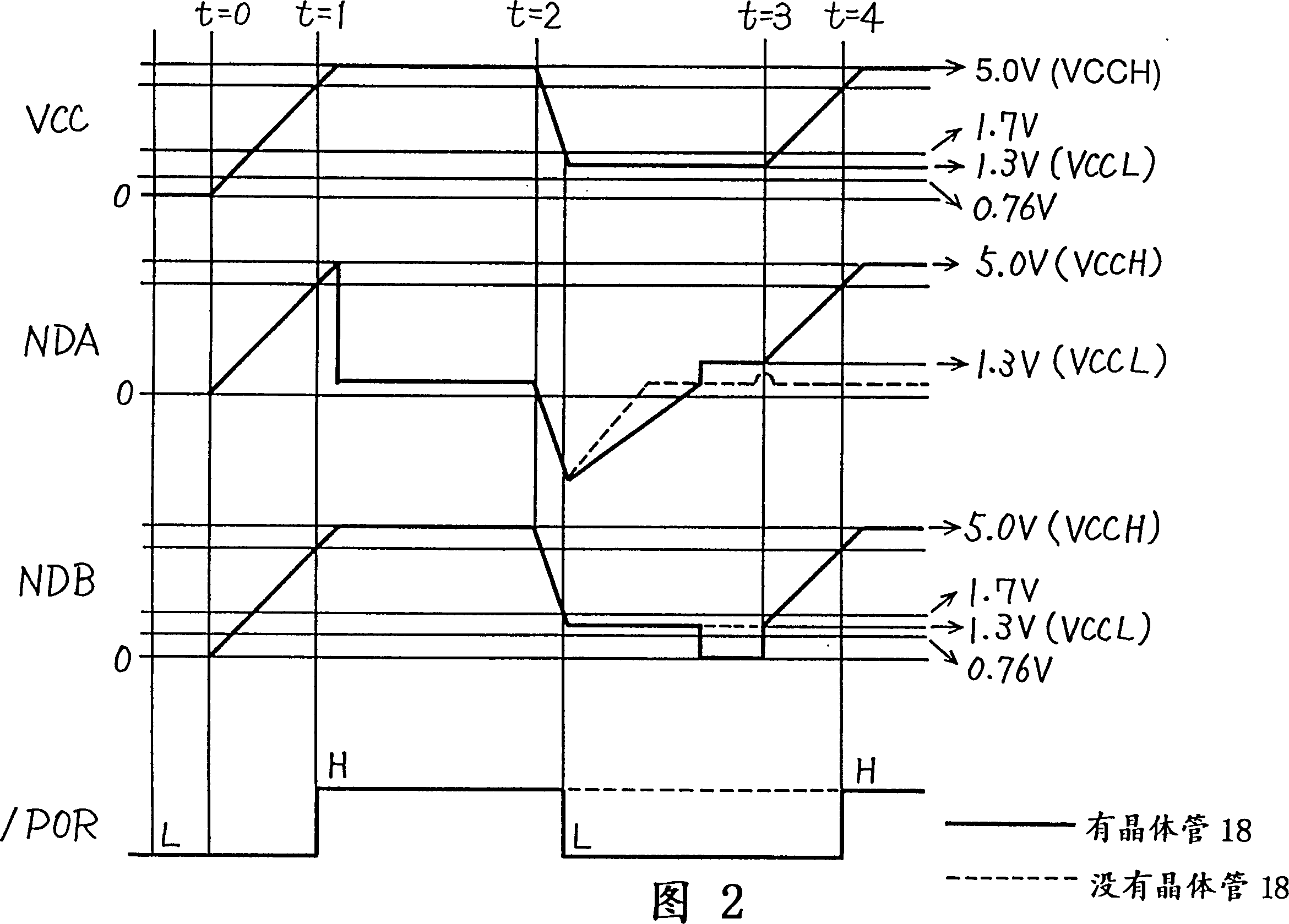
[0041] In the above-mentioned Embodiment 1, one N-channel MOS transistor 18 is provided, so the voltage value is fixed to the voltage value (1.7 V in Embodiment 1) that activates the power-on reset signal / POR, however, the voltage value It may also be adjusted according to the specifications of the semiconductor integrated circuit device using the power-on reset circuit.
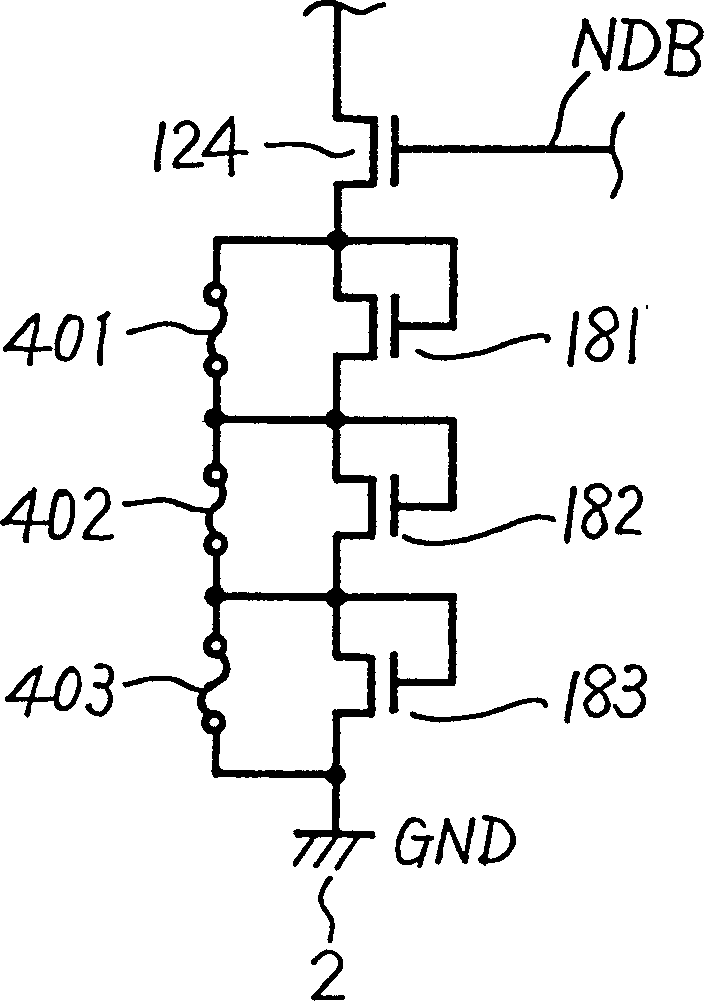
[0042] image 3 It is a diagram showing the configuration of main parts of the power-on reset circuit of the second embodiment for the purpose of adjusting the above-mentioned voltage value. refer to image 3 , in this embodiment 2, instead of the N-channel MOS transistor 18 of the above-mentioned embodiment 1, three N-channel MOS transistors 181 to 181 are connected in series between the source of the N-channel MOS transistor 124 and the ground node 2 183. The respective N-channel MOS transistors 181 to 183 are connected in the form of diodes. Further, fuses 401 to 403 as switching elements are connected...
Embodiment 3
[0046] In the above-mentioned second embodiment, the voltage value of the power-on-reset signal / POR can be adjusted artificially according to the power supply voltage, but the voltage value can also be automatically adjusted according to the power supply voltage VCC.
[0047] 4 is a circuit diagram showing a configuration of main parts of a power-on-reset circuit according to a third embodiment for automatically adjusting a voltage value for activating a power-on-reset signal / POR according to a power supply voltage VCC. Referring to FIG. 4 , in this third embodiment, N-channel MOS transistors 411 to 413 are connected as switching elements instead of the fuses 401 to 403 of the above-mentioned second embodiment. In addition, resistors 431 to 434 are connected in series between the power supply node 1 and the ground node 2, and the connection nodes ND1 to ND3 of the resistors 431 to 434 are connected to the gates of the N-channel MOS transistors 411 to 413, respectively. Inver...
PUM
 Abstract
Description
Claims
Application Information