igbt device and its manufacturing method

A manufacturing method and device technology, applied in semiconductor/solid-state device manufacturing, semiconductor devices, electrical components, etc., can solve the problems of large current, increase the total concentration, accelerate the recombination speed of electrons and holes, and alleviate the problem of current concentration Effect

Active Publication Date: 2022-01-11
GTA SEMICON CO LTD
View PDF7 Cites 0 Cited by
  • Summary
  • Abstract
  • Description
  • Claims
  • Application Information

AI Technical Summary

Problems solved by technology

[0003] In view of the above-mentioned shortcomings of the prior art, the purpose of the present invention is to provide an IGBT device and its manufacturing method, which is used to solve the problem of excessive current in the transition region when the IGBT is turned off in the prior art

Method used


Image

  • igbt device and its manufacturing method
  • igbt device and its manufacturing method
  • igbt device and its manufacturing method

Examples


Embodiment 1

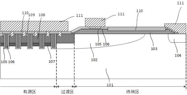
[0034] The IGBT device can be divided into three areas, namely active regions, transition zones, and terminal districts, respectively. When the IGBT device is turned on, the back P-type collector begins to inject holes into the drift zone of the IGBT device. During the IGBT device shutdown, it is necessary to inject all the electrons and holes in the drift area during the transfer, and electrons from IGBT devices. The back is out, and the holes flow out from the front side of the IGBT device. The hole in the active region can flow directly from the frontal opening of the active region, but the front side of the terminal area does not currently flow, the hole of the terminal area mainly flows from the opening of the transition zone, which can cause a current in the transition zone. Concentration issues, the transition concentration of local currents, resulting in rising local temperatures, reducing the reliability of IGBT devices.

[0035] In order to solve the above problem, if Fi...

Embodiment 2

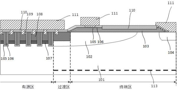
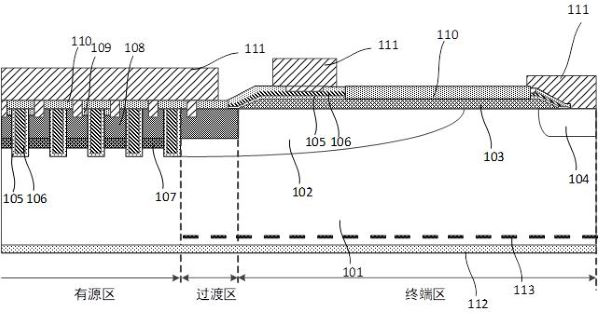
[0050] like Figure 5 As shown, the present embodiment provides an IGBT device comprising: a substrate 101, the substrate 101 comprising a relative first main surface and a second main surface, the first main surface forming an IGBT device The front structure includes a active region, a transition region, and a terminal region; an oxygen ion abduction layer 113 is formed in the second main surface of the transition zone and terminal region; the collector region 112 is formed in the The second main surface of the substrate 101; the hydrogen ion doping region 114 is formed in the second main surface of the substrate 101, and the oxygen ion defective layer 113 is located within the hydrogen ion doped region 114; The oxygen ions defective layer 113 reduces the hole life of the transition zone and the terminal region, while the oxygen ion of the oxygen ion abduction layer 113 is used as the adsorbent of the hydrogen ion to increase the hydrogen ion in the hydrogen ion doped region 114. ...


PUM


Abstract

The invention provides an IGBT device and a manufacturing method thereof. The IGBT device includes: a substrate, the substrate includes opposite first main surfaces and second main surfaces, the first main surface is formed with a front structure of the IGBT device, and the IGBT device includes The active region, the transition region and the terminal region; the oxygen ion defect layer, formed in the second main surface of the transition region and the terminal region; the collector region, formed on the second main surface of the substrate; the hydrogen ion doped region, formed In the second main surface of the substrate, the oxygen ion defect layer is located in the hydrogen ion doped region, wherein the oxygen ions in the oxygen ion defect layer serve as adsorbents for hydrogen ions so as to increase the doping of hydrogen ions in the hydrogen ion doped region. impurity concentration. The present invention reduces the emission efficiency of the transition region and the terminal region when the IGBT device is turned on, and at the same time increases the recombination speed of electrons and holes in the transition region and the terminal region when the IGBT device is turned off, thereby effectively alleviating the current concentration problem existing in the transition region , Improve the reliability of the IGBT chip.

Description

Technical field [0001] The present invention belongs to the design and manufacturing of semiconductor integrated circuits, and, in particular, to an IGBT device and a method of fabricating thereof. Background technique [0002] IGBT (insulated gate bipolar transistor) is a composite full-controlled voltage driving power semiconductor device consisting of BJT (bipolarized triode) and MOSFET (insulated gate field effect tube), so it has a MOSFET input impedance high. The driving circuit is small, the driving is simple, the switching speed is fast, and the switch loss is small, and the BJT current density is high, the current is strong, the current reduction is strong, and the turning on saturation pressure is reduced. Since the inventions in the early 1980s, it has been widely studied at home and abroad. At present, IGBT has broad application prospects, widely used in new energy vehicles, industrial frequency conversion, photovoltaic, smart grids and locomotives, etc. With the cont...

Claims


Application Information

Patent Timeline
Patent Type & Authority Patents(China)
IPC IPC(8): H01L21/331H01L29/739H01L29/36H01L21/266
CPCH01L29/66348H01L29/7397H01L29/36H01L21/266
Inventor 曹功勋
Owner GTA SEMICON CO LTD
Why Eureka
Try Eureka