IGBT device and manufacturing method thereof

A manufacturing method and device technology, applied in semiconductor/solid-state device manufacturing, semiconductor devices, electrical components, etc., can solve problems such as large current, achieve the effects of increasing the total concentration, accelerating the recombination speed of electrons and holes, and alleviating current concentration

Active Publication Date: 2021-10-29
GTA SEMICON CO LTD
View PDF7 Cites 1 Cited by
  • Summary
  • Abstract
  • Description
  • Claims
  • Application Information

AI Technical Summary

Problems solved by technology

[0003] In view of the above-mentioned shortcomings of the prior art, the purpose of the present invention is to provide an IGBT device and its manufacturing method, which is used to solve the problem of excessive current in the transition region when the IGBT is turned off in the prior art

Method used


Image

  • IGBT device and manufacturing method thereof
  • IGBT device and manufacturing method thereof
  • IGBT device and manufacturing method thereof

Examples


Embodiment 1

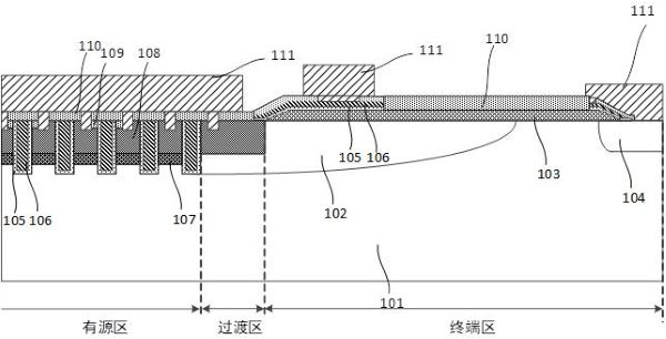
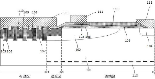
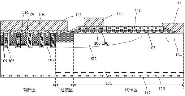
[0034] The IGBT device can be divided into three regions, namely the active region, the transition region and the termination region. When the IGBT device is turned on, the P-type collector on the back side begins to inject holes into the drift region of the IGBT device. The holes flow out from the back side of the IGBT device, and the holes flow out from the front side of the IGBT device. The holes in the active region can flow out directly from the front opening of the active region, but there is no current channel on the front side of the termination region, and the holes in the termination region mainly flow out from the opening in the transition region, which will cause current flow in the transition region Concentration problem, the transitional concentration of local current leads to local temperature rise and reduces the reliability of IGBT devices.

[0035] In order to solve the above problems, such as Figure 1~Figure 5 As shown, the present embodiment provides a ma...

Embodiment 2

[0050] like Figure 5 As shown, this embodiment provides an IGBT device, the IGBT device includes: a substrate 101, the substrate 101 includes an opposite first main surface and a second main surface, and the first main surface is formed with an IGBT device The front structure of the IGBT device includes an active region, a transition region and a termination region; an oxygen ion defect layer 113 is formed in the second main surface of the transition region and termination region; a collector region 112 is formed in the The second main surface of the substrate 101; the hydrogen ion doped region 114 is formed in the second main surface of the substrate 101, and the oxygen ion defect layer 113 is located in the hydrogen ion doped region 114; through the The oxygen ion defect layer 113 reduces the hole lifetime of the transition region and the terminal region, and at the same time, the oxygen ion in the oxygen ion defect layer 113 acts as an adsorbent of hydrogen ions, thereby i...


PUM


Abstract

The invention provides an IGBT device and a manufacturing method thereof. The IGBT device comprises a substrate, an oxygen ion defect layer, a collector region and a hydrogen ion doped region; the substrate comprises a first main surface and a second main surface which are opposite to each other, a front surface structure of the IGBT device is formed on the first main surface, and the IGBT device comprises an active region, a transition region and a terminal region; the oxygen ion defect layer is formed in the second main surface of the transition region and the terminal region; the collector region is formed on the second main surface of the substrate; the hydrogen ion doped region is formed in the second main surface of the substrate, the oxygen ion defect layer is located in the hydrogen ion doped region, and oxygen ions of the oxygen ion defect layer serve as adsorbents of the hydrogen ions, so that the doping concentration of the hydrogen ions in the hydrogen ion doped region is increased. When the IGBT device is switched on, the emission efficiency of the transition region and the terminal region is reduced, and when the IGBT device is switched off, the electron and hole recombination speed of the transition region and the terminal region is improved, so that the problem of current concentration in the transition region is effectively relieved, and the reliability of an IGBT chip is improved.

Description

technical field [0001] The invention belongs to the field of semiconductor integrated circuit design and manufacture, and in particular relates to an IGBT device and a manufacturing method thereof. Background technique [0002] IGBT (Insulated Gate Bipolar Transistor) is a composite fully-controlled voltage-driven power semiconductor device composed of BJT (Bipolar Transistor) and MOSFET (Insulated Gate Field Effect Transistor), so it has both MOSFET input impedance and high , The driving circuit has the advantages of low power, simple driving, fast switching speed, and small switching loss, and has the advantages of large current density, strong current handling capability, and low conduction saturation voltage of BJT. Since its invention in the early 1980s, it has been widely studied at home and abroad. At present, IGBT has broad application prospects and is widely used in new energy vehicles, industrial frequency conversion, photovoltaics, smart grids and locomotives. Wit...

Claims


Application Information

Patent Timeline
Patent Type & Authority Applications(China)
IPC IPC(8): H01L21/331H01L29/739H01L29/36H01L21/266
CPCH01L29/66348H01L29/7397H01L29/36H01L21/266
Inventor 曹功勋
Owner GTA SEMICON CO LTD
Why Eureka
Try Eureka