Preparation method of double-sided MWT-HIT battery assembly
A battery module, double-sided technology, applied in electrical components, circuits, photovoltaic power generation and other directions, can solve the problems of poor cost performance, difficult to achieve low-cost double-sided, and high unit price of low-temperature silver paste consumption, to reduce consumption, reduce kWh cost and the effect of improving comprehensive power generation
- Summary
- Abstract
- Description
- Claims
- Application Information
AI Technical Summary
Problems solved by technology
Method used
Image
Examples
Embodiment 1
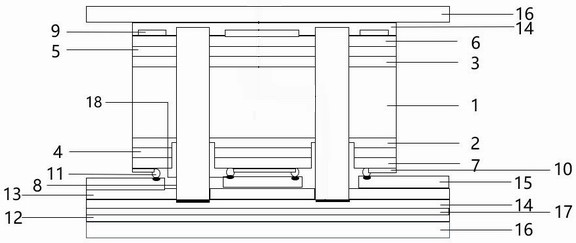
[0059] This embodiment is a double-sided MWT-HIT battery assembly, which sequentially includes front ultra-clear high-transparency glass, front packaging polymer, front electrode, front TCO layer, front N+ type doped amorphous silicon layer, front Intrinsic amorphous silicon passivation layer, N-type single crystal silicon substrate, back intrinsic amorphous silicon passivation layer, back P-type doped amorphous silicon emitter layer, back TCO layer, back electrode ring, second back conductive Foil, second high-transparency insulating polymer on the back, first conductive foil on the back, color-changing film on the back, first high-transparency insulating polymer on the back, and ultra-clear high-transparency glass on the back. The fine grid pattern on the back of the battery has the same height as the front graphic, and the fine grid pattern on the back is only designed as a ferrule at the electrode point, forming a back electrode ring surrounding the positive electrode point...
Embodiment 2
[0070] On the other hand, the present invention simultaneously provides a process preparation method of a double-sided MWT-HIT battery assembly, the process preparation method comprising the following process steps:
[0071] S01 performs laser drilling on N-type silicon wafers;
[0072] S02 silicon wafer cleaning and polishing: texture and clean the N-type monocrystalline silicon substrate to remove the mechanical damage layer and pollutants on the surface of the silicon substrate to form a pyramid texture;
[0073] S03 depositing an intrinsic amorphous silicon layer on both sides;
[0074] N-type amorphous silicon deposition is performed on the front of S04;
[0075] P-type amorphous silicon deposition on the back of S05;
[0076] TCO deposition on the front side of S06;
[0077] TCO deposition on the back of S07;
[0078] On the back of S08, print etching paste around the position of the hole to partially etch the TCO and P-type amorphous silicon on the back;
[0079] S...
Embodiment 3
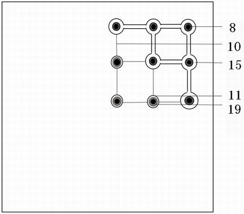
[0086] The present application also provides an integrated composite localized conductive core board. In order to ensure a clearer description of the embodiments of the present invention, the following description is made. by figure 2 For example, figure 2 The back view of the MWT-HIT battery. The integrated composite local conductive core board in the present invention is mainly in contact with the back of the MWT-HIT battery and laminated and packaged. Before the alignment contact lamination package needs to be in figure 2 Conductive glue is printed on the back negative pole and the back positive electrode ring respectively as shown in . The covering of each layer is then carried out in the following order.
[0087] 1. Covered by the second conductive foil on the back, the ring-shaped area in the second back conductive foil completely covers the positive electrode ring on the back, and conducts effective connection and conduction through the conductive glue on the pos...
PUM
 Abstract
Description
Claims
Application Information


