Thin-film solar cell

A solar cell and thin film technology, applied in circuits, photovoltaic power generation, electrical components, etc., can solve the problems of fragility, troublesome production process, inability to manufacture and process, and achieve the effect of wide selectivity

Pending Publication Date: 2021-11-09
侯勋添
View PDF7 Cites 0 Cited by
  • Summary
  • Abstract
  • Description
  • Claims
  • Application Information

AI Technical Summary

Problems solved by technology

[0002] Among solar cells, the main material of thin-film solar cells is light and thin, so it saves materials, but its photoelectric conversion efficiency is low. If the photoelectric conversion efficiency can be improved, its economic value will be increased by virtue of its low cost advantage
[0003] Traditional thin-film solar cells, such as p-i-n type silicon thin-film solar cells, have very fine craftsmanship and manufacturing, so traditional solar cells must be very flat from the glass substrate to be absolutely flat, otherwise they cannot be manufactured and processed. Glass is used as the substrate, but this kind of glass substrate is not an ordinary glass material, and its production process is troublesome, and the larger the area, the higher the technical requirements, so it is expensive and fragile
In addition, the rigidity of the glass substrate is the main reason why the solar cell cannot be made flexible, and because it is not flexible, the installation site is fixed, it is not suitable for use in places that require curved surfaces, and it cannot resist strong winds, heavy rain or External forces such as ocean waves, these external forces are likely to break and damage the glass substrate of the solar cell and make it unusable, so its application is limited

Method used


Image

  • Thin-film solar cell
  • Thin-film solar cell
  • Thin-film solar cell

Examples


Embodiment Construction

[0036] In order to have a further understanding of the features and features of the present invention, the following preferred embodiments are now listed and described as follows in conjunction with the accompanying drawings:

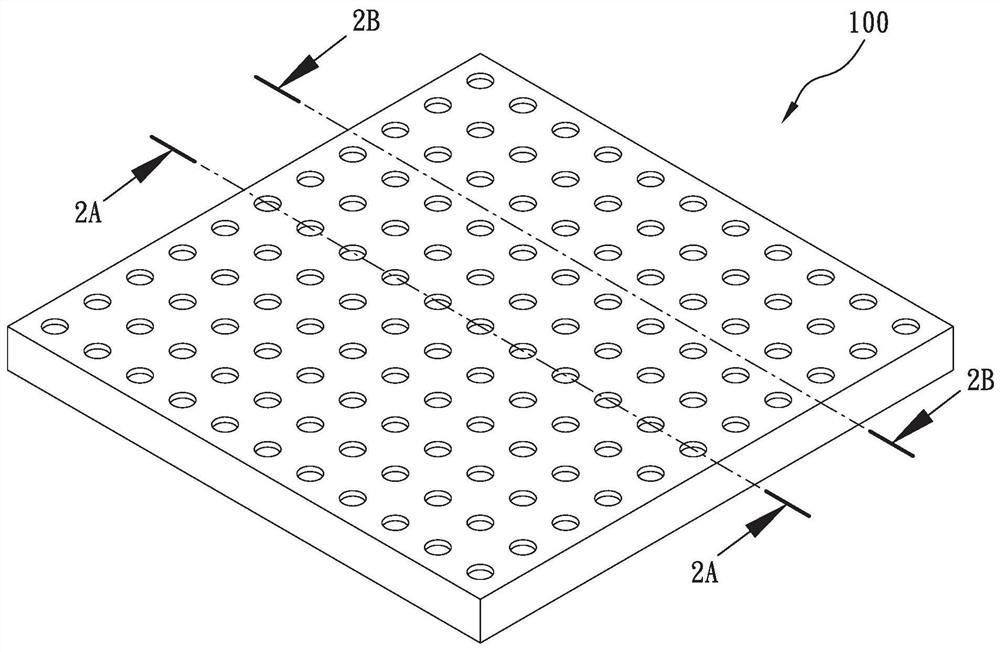
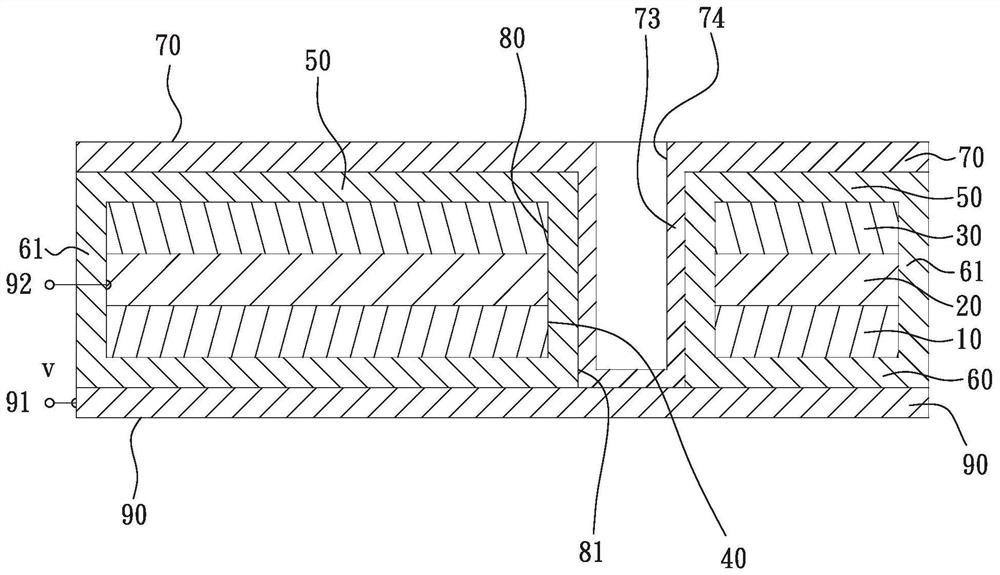
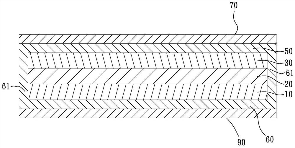
[0037] In the following examples, figure 1 There are multiple perforations 40, for ease of illustration, Fig. 2~ Figure 7 The perforation 40 in is only drawn as an example. see figure 1 2A and 2B, a preferred embodiment of the thin film solar cell 100 of the present invention includes a mirror material layer 10, a contact conductive layer 20, an NP-type semiconductor lower layer 30, a plurality of through holes 40, a NP Type semiconductor upper layer 50, an insulating layer 60, a plurality of insulators 80, a transparent conductive layer 70, a conductive substrate 90, a plurality of conductors 73 and other stacked layers and components.

[0038] see Figure 3a ~ Figure 3f Shown is a process step chart of an embodiment of the thin film solar cell ...


PUM


Abstract

The invention provides a thin-film solar cell, which can solve the problem that a solar cell taking a stainless steel foil as a back connection conductive material can only use an amorphous silicon thin-film semiconductor and cannot be suitable for other semiconductor materials. The thin-film solar cell comprises the following laminated layers and components: a conductive substrate, an insulating layer, a mirror surface material layer, a contact conductive layer, an NP type semiconductor lower layer, an NP type semiconductor upper layer and a transparent conductive layer, and is provided with a plurality of through holes, a through insulator and a conductor, wherein the through holes penetrate through the mirror surface material layer, the contact conductive layer and the NP type semiconductor lower layer, the insulator is arranged in the through hole and is connected with the NP type semiconductor upper layer and the insulating layer, the conductor is arranged in the through insulator to be electrically connected with the transparent conductive layer and the conductive substrate, charges can be output by the conductive substrate and the mirror surface material layer, and various semiconductor materials can be used through selection of matching materials of the contact conductive layer and the NP type semiconductor lower layer.

Description

technical field [0001] The invention relates to a thin-film solar cell, in particular to a thin-film solar cell with multiple through-hole conduction paths. Background technique [0002] Among solar cells, the main material of thin-film solar cells is light and thin, so it saves materials, but its photoelectric conversion efficiency is low. If the photoelectric conversion efficiency can be improved, its economic value will be increased by virtue of its low cost advantage. [0003] Traditional thin-film solar cells, such as p-i-n type silicon thin-film solar cells, have very fine craftsmanship and manufacturing, so traditional solar cells must be very flat from the glass substrate to be absolutely flat, otherwise they cannot be manufactured and processed. Glass is used as the substrate, but this kind of glass substrate is not an ordinary glass material, and its production process is troublesome, and the larger the area, the higher the technical requirements, so it is expensiv...

Claims


Application Information

Patent Timeline
Patent Type & Authority Applications(China)
IPC IPC(8): H01L31/073H01L31/0749H01L31/0224H01L31/0445H02S30/20
CPCH01L31/073H01L31/0749H01L31/022425H01L31/0445H02S30/20Y02E10/541Y02E10/543
Inventor 侯勋添
Owner 侯勋添
Why Eureka
Try Eureka