MEMS silicon-based membrane hole atomizing core and manufacturing method thereof

A manufacturing method and atomizing core technology, applied in tobacco and other directions, can solve the problems of poor process controllability, easy liquid frying, uneven heating, etc., to reduce the difficulty of opening holes, control the manufacturing process, and solve the problem of local overheating. Effect

Pending Publication Date: 2021-11-16
美满芯盛(杭州)微电子有限公司
View PDF0 Cites 2 Cited by
  • Summary
  • Abstract
  • Description
  • Claims
  • Application Information

AI Technical Summary

Problems solved by technology

[0005] At present, the atomizing core has the following disadvantages: 1. The porous aperture of the ceramic atomizing core is inconsistent, resulting in uneven heating and local overheating and carbonization; 2. The thermal conductivity of ceramic materials is poor, resulting in slow atomization speed; 3. Silicon-based The atomizing core, due to thickness and process limitations, has a large diameter and a straight hole, resulting in inability to lock liquid and poor liquid storage performance; 4. The existing silicon-based atomizing core has high thermal conductivity and directly contacts the liquid storage tank 5. The existing porous silicon atomization core scheme also has the problems of poor process controllability and inconsistent pore size, resulting in uneven heating and local overheating and carbonization

Method used


Image

  • MEMS silicon-based membrane hole atomizing core and manufacturing method thereof
  • MEMS silicon-based membrane hole atomizing core and manufacturing method thereof
  • MEMS silicon-based membrane hole atomizing core and manufacturing method thereof

Examples


Embodiment 1

[0063] S01: preparing a silicon substrate sheet 1 with a thickness of 300 μm;

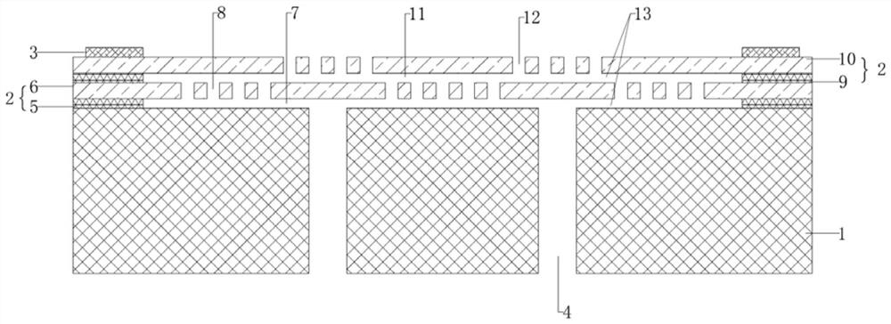
[0064] S02: using PECVD method, depositing a first layer of silicon oxide 5 on the silicon substrate 1, and depositing a first layer of polysilicon 6 on the first layer of silicon oxide 5;

[0065] S03: performing photolithography and etching on the first layer of polysilicon 6 to etch the primary atomization hole 8;

[0066] S04: Deposit a second layer of silicon oxide 9 on the first layer of polysilicon 6 by PECVD, and deposit a second layer of polysilicon 10 on the second layer of silicon oxide 9;

[0067] S05: Deposit a metal electrode 3 on the second layer of polysilicon 10, the deposited metal is Ti / Au, and make a specific pattern through a dry etching process;

[0068] S06: performing photolithography and etching on the second layer of polysilicon 10 to etch out secondary atomization holes 12;

[0069] S07: performing photolithography and etching on the back side of the silicon substrate 1...

Embodiment 2

[0072] S01: preparing a silicon substrate sheet 1 with a thickness of 300 μm;

[0073] S02: using LPCVD method, depositing a first layer of silicon oxide 5 on the silicon substrate 1, and depositing a first layer of polysilicon 6 on the first layer of silicon oxide 5;

[0074] S03: performing photolithography and etching on the first layer of polysilicon 6 to etch the primary atomization hole 8;

[0075] S04: Deposit a second layer of silicon oxide 9 on the first layer of polysilicon 6 by using LPCVD, and deposit a second layer of polysilicon 10 on the second layer of silicon oxide 9;

[0076] S05: Deposit a metal electrode 3 on the second layer of polysilicon 10, the deposited metal is Ti / TiN / Pt, and make a specific pattern through a wet etching process;

[0077] S06: performing photolithography and etching on the second layer of polysilicon 10 to etch out secondary atomization holes 12;

[0078] S07: performing photolithography and etching on the back side of the silicon s...

Embodiment 3

[0081] S01: Prepare a silicon substrate sheet 1 with a thickness of 400 μm;

[0082] S02: using PECVD method, depositing a first layer of silicon oxide 5 on the silicon substrate 1, and depositing a first layer of polysilicon 6 on the first layer of silicon oxide 5;

[0083] S03: performing photolithography and etching on the first layer of polysilicon 6 to etch the primary atomization hole 8;

[0084] S04: Deposit a second layer of silicon oxide 9 on the first layer of polysilicon 6 by using LPCVD, and deposit a second layer of polysilicon 10 on the second layer of silicon oxide 9;

[0085] S05: Deposit a metal electrode 3 on the second layer of polysilicon 10, the deposited metal is Ti / Au, and make a specific pattern through a dry etching process;

[0086] S06: performing photolithography and etching on the second layer of polysilicon 10 to etch out secondary atomization holes 12;

[0087] S07: performing photolithography and etching on the back side of the silicon substra...


PUM

PropertyMeasurementUnit
thicknessaaaaaaaaaa
thicknessaaaaaaaaaa

Abstract

The invention discloses an MEMS silicon-based membrane hole atomizing core, and belongs to the technical field of liquid heating atomizing cores, the MEMS silicon-based membrane hole atomizing core comprises a silicon substrate slice, at least one layer of membrane hole mechanism and a metal electrode, the at least one layer of membrane hole mechanism is fixedly connected to the top surface of the silicon substrate slice, and the metal electrode is fixedly connected to the top of the membrane hole mechanism. At least one liquid guide hole is formed in the silicon substrate slice, and the liquid guide hole is communicated with the bottom of the silicon substrate slice and the top of the film hole mechanism; a multi-layer film hole mechanism is adopted, decomposition of the overall thickness is facilitated, the hole opening thickness of a first-stage atomization hole or a second-stage atomization hole is reduced, the hole opening difficulty of the atomization hole is reduced, small-aperture non-straight-through hole opening of the atomization hole is achieved, so that good liquid locking and storing functions are achieved; and the opening manufacturing process of the atomization holes is controllable, the consistency is high, the uniformity is good, and the problems of local overheating and dry burning carbonization are solved.

Description

technical field [0001] The invention belongs to the technical field of liquid heating atomizing cores, and in particular relates to a MEMS silicon-based membrane hole atomizing core and a manufacturing method thereof. Background technique [0002] As the core component of the liquid vaporization device, the heat-generating atomizing element heats the liquid and turns it into mist-like aerosol, which is inhaled by the user. In order to ensure a good taste for the smoker, it is required that the atomization element heat the atomized liquid to be fast, uniform, consistent, delicate and minimize the generation of harmful substances. There are two main types of heating atomizing cores for existing liquid atomizing devices. The first ceramic atomizing core has a mature technical solution and is the solution adopted by mainstream products at present. It is composed of ceramics and heating electrodes. The ceramics are sintered at high temperature. It is made into a bowl-shaped stru...

Claims


Application Information

Patent Timeline
Patent Type & Authority Applications(China)
IPC IPC(8): A24F40/46A24F40/485A24F40/70
Inventor 王敏锐
Owner 美满芯盛(杭州)微电子有限公司
Why Eureka
Try Eureka