Interleaved Memory Pseudo-Random Mapping Method for Parallel Computing

A mapping method and parallel computing technology, applied in the field of memory, can solve the problems that different address lengths cannot be flexibly expanded, and the realization circuit is complicated, and achieve the effect of improving parallel access and parallel computing performance, easy design, and improving parallel storage performance.

Active Publication Date: 2022-03-25
HEXAFLAKE (NANJING) INFORMATION TECH CO LTD
View PDF12 Cites 0 Cited by
  • Summary
  • Abstract
  • Description
  • Claims
  • Application Information

AI Technical Summary

Problems solved by technology

[0007] In the above scheme, there are disadvantages such as complex circuit implementation, independent transformation matrix for forward and reverse transformation, and inability to flexibly expand for different address lengths.

Method used


Image

  • Interleaved Memory Pseudo-Random Mapping Method for Parallel Computing
  • Interleaved Memory Pseudo-Random Mapping Method for Parallel Computing
  • Interleaved Memory Pseudo-Random Mapping Method for Parallel Computing

Examples


Embodiment 1

[0110] Suppose the interleaved memory contains 8 memory blocks, namely M=3, B=2 M =8; the block address of each storage block is K=29 bits. So the full address of the entire interleaved memory is M+K=32 bits.

[0111] S1: Since B-1≤M+K, there is no need to divide M;

[0112] S2: Use M=3 as the order to check the table of commonly used primitive polynomials to obtain the primitive polynomial F(x)=x 3 +x+1;

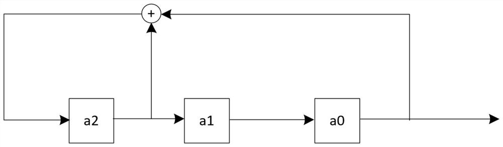
[0113] S3: The linear feedback shift register circuit corresponding to F(x) is as follows figure 1 .

[0114] Set the initial states of the three shift registers {a2,a1,a0}={0,0,1}, by shifting 6 times and adding the initial state, 7 groups of shift register states that do not repeat can be obtained, respectively {0,0,1}, {1,0,0}, {1,1,0}, {1,1,1}, {0,1,1}, {1,0,1}, {0 ,1,0}; Thus, each state as a column can form an H matrix with 3 rows and 7 columns, namely:

[0115] column 6 column 5 column 4 column 3 column 2 column 1 column 0 0 1 0 1 ...

Embodiment 2

[0126] Assume that the interleaved memory includes 128 memory blocks, ie M=7, B=2M=128; the address within the block of each memory block is K=25 bits. So the full address of the entire interleaved memory is M+K=32 bits.

[0127] S1: Since B-1>M+K, it is necessary to divide M, here M is divided into two parts, let M 1 = 4, M 2 = 3, then B 1 =16,B 2 = 8;

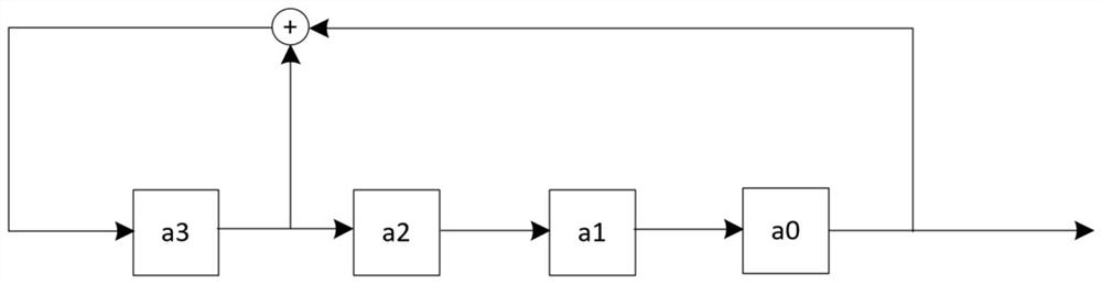
[0128] S2: Use M 1 and M 2 As the order, look up the primitive polynomial table to get the primitive polynomial F 1 (x)=x 4 +x+1 and F 2 (x)=x 3 +x+1.

[0129] S3: According to F 1 (x) and F 2 (x) corresponds to the linear feedback shift register circuit (respectively as figure 2 with image 3 shown), get H 1 and H 2 matrix.

[0130] h 1 matrix:

[0131] column 14 column 13 column 12 column 11 column 10 column 9 column 8 column 7 column 6 column 5 column 4 column 3 column 2 column 1 column 0 0 0 1 0 0 1 1 0 1 0 1 1 1 1 0 0 1 0 0 1 1 0 1 0 ...


PUM


Abstract

The invention discloses a cross-memory pseudo-random mapping method for parallel computing. The pseudo-random sequence generated by the maximum sequence code (m-sequence) is used to form an address mapping matrix, which can improve the performance of parallel access and parallel computing, and slow down Store latency in dynamic memory. The present invention adopts an H matrix adjustment method of address mapping, overcomes the weakness of the previous method, and ensures that the same H matrix can be used for forward mapping and reverse mapping. The address mapping matrix generated by the invention is combined with the XOR function to form an address mapping circuit, which is easy to design and simple in structure. For different address widths, the present invention uses an address division mapping method to optimize the pseudo-randomness of the mapping matrix to improve parallel storage performance.

Description

technical field [0001] The invention relates to the field of memory, in particular to the field of chip design and computer architecture, in particular to a pseudo-random mapping method for cross-memory for parallel computing. Background technique [0002] Machine learning, scientific computing and graphics processing require huge computing power, which is generally provided by large chips (such as GPU, TPU, APU, etc.) to achieve highly complex machine learning tasks and graphics processing tasks. Using machine learning to do recognition requires a huge deep learning (Deep Learning) network and massive image data, and the training process is very time-consuming; in a 3D application or game scene, if recursive ray-tracing (Recursive Ray-Tracing) rendering is used, and Complex scenes require massive calculations. This requires extremely high computing performance and storage bandwidth. On the other hand, machine learning and big data processing algorithms often require a lar...

Claims


Application Information

Patent Timeline
Patent Type & Authority Patents(China)
IPC IPC(8): G06F3/06G06F7/58G06F17/16
CPCG06F3/0631G06F3/0613G06F3/064G06F7/582G06F17/16
Inventor 赵鹏侯红朝王东辉葛建明满新攀桑永奇姚飞
Owner HEXAFLAKE (NANJING) INFORMATION TECH CO LTD
Why Eureka
Try Eureka