
Single-ended input pseudo-differential ultra-wideband transistor amplifier

A single-ended input, amplifier technology, used in differential amplifiers, DC-coupled DC amplifiers, amplifiers, etc., can solve problems such as reduced efficiency, difficult use of RF amplifiers, and inability to provide ultra-wideband amplification performance, to improve stability, improve Effects of low frequency characteristics

Active Publication Date: 2021-11-16
SOUTHEAST UNIV
View PDF2 Cites 0 Cited by
  • Summary
  • Abstract
  • Description
  • Claims
  • Application Information

AI Technical Summary

Problems solved by technology

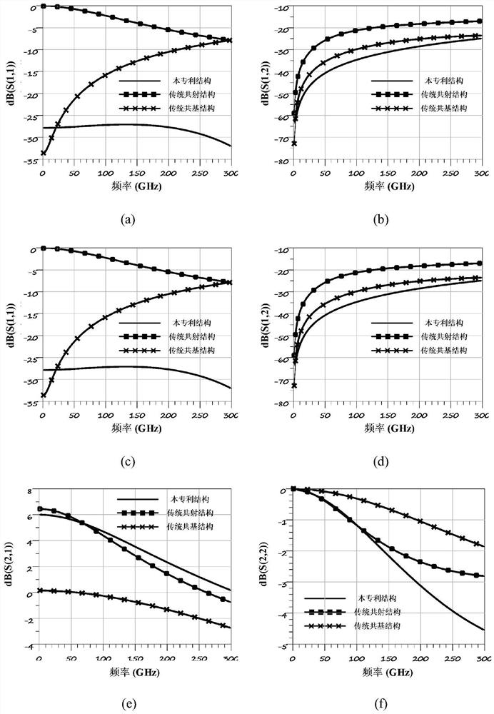
However, for traveling wave amplifiers, since a large number of transistors are required for single-stage amplification, this will lead to increased power consumption and reduced efficiency, and usually cannot provide ultra-wideband amplification performance such as DC to 200GHz or greater bandwidth
As for the common base (gate) amplifier structure amplifier, although this structure can provide better input matching at low frequency output, due to the influence of transistor physical characteristics and parasitic parameters, it still cannot provide excellent performance in the ultra-high frequency range. The input matching performance of
At the same time, in order to ensure normal operation, traditional RF amplifiers often require many bypass capacitors and DC blocking capacitors, which also makes it difficult for traditional RF amplifiers to be used at low frequencies.

Method used


Image

  • Single-ended input pseudo-differential ultra-wideband transistor amplifier
  • Single-ended input pseudo-differential ultra-wideband transistor amplifier
  • Single-ended input pseudo-differential ultra-wideband transistor amplifier

Examples


Embodiment Construction

[0024] Below in conjunction with accompanying drawing, the present invention will be further described

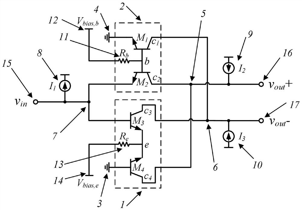
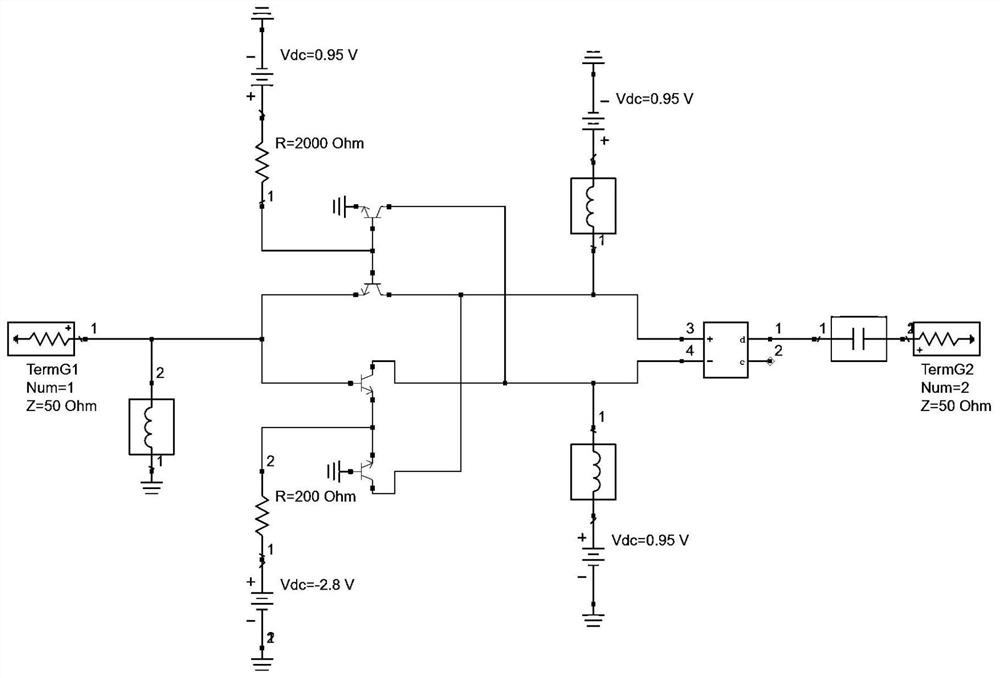
[0025] Such as figure 1 As shown, a single-end input pseudo-differential UWB transistor amplifier topology of the present invention is a single-end input pseudo-differential UWB transistor amplifier structure.

[0026] Including one differential common-emitter structure amplifier 1, one differential common-base structure amplifier 2, the ground input terminal 3 of the differential common-emitter structure amplifier, and the ground input terminal 4 of the differential common-base structure amplifier are directly grounded, and the differential common-emitter structure The non-inverting input terminal 7 of the amplifier 1 is connected to the non-inverting input terminal of the differential common-base structure amplifier 2, and the non-inverting output terminal 5 of the differential common-emitter structure amplifier 1 is connected to the non-inverting output terminal of the d...


PUM


Abstract

The invention discloses a single-ended input pseudo-differential ultra-wideband transistor amplifier, and the amplifier comprises a differential common-emitter structure amplifier (1) and a differential common-base structure amplifier (2). A grounding input end (3) of the differential common-emitter amplifier and a grounding input end (4) of the differential common-base amplifier are directly grounded, in-phase input ends (7) of the two amplifiers are connected, in-phase output ends (5) of the two amplifiers are connected, and inverted output ends (6) of the two amplifiers are connected; the base (b) of the differential common-base amplifier is connected with a common-mode resistor Rb (11), and the emitter (e) of the differential common-emitter amplifier is connected with a common-mode resistor Re (13). One of the differential input ends is grounded, and the common-mode resistor is used for suppressing a common-mode signal, so that the problems that a traditional pseudo-differential structure is poor in common-mode suppression characteristic, and bandwidth is reduced due to the fact that a bypass and a blocking capacitor are needed are solved, and the ultra-wideband input matching and amplifying characteristic from direct current to radio frequency is achieved.

Description

technical field [0001] The invention relates to a novel single-ended input pseudo-differential ultra-wideband transistor amplifier structure, specifically an amplifier structure that is manufactured by semiconductor integrated circuit technology and uses transistors to amplify radio frequency signals, so as to realize ultra-wideband signals from direct current to radio frequency Amplification matches the input. Background technique [0002] UWB RF amplifier is one of the core modules of RF measurement instruments and UWB communication systems, and its performance directly affects the performance of RF instruments and equipment and the communication speed of UWB communication systems. With the further development of radio technology, the frequency band covered by current radio frequency technology is getting wider and wider, covering from low frequency band to millimeter wave frequency band, and is evolving to terahertz frequency band, which is suitable for the bandwidth of u...

Claims


Application Information

Patent Timeline
Patent Type & Authority Applications(China)
IPC IPC(8): H03F1/48H03F3/19H03F3/45
CPCH03F1/48H03F3/19H03F3/45076H03F2200/451H03F2200/36
Inventor 洪伟唐大伟李泽坤周培根
Owner SOUTHEAST UNIV
Learn More