Micro-etching processing technology for resin plug hole of dry film cover

A resin plug hole, processing technology, applied in printed circuits, electrical components, and chemical/electrolytic methods to remove conductive materials, etc., can solve problems such as uneven orifices, missing copper in the orifices, and small board line widths. To achieve the effect of good quality, good effect and smooth orifice

Active Publication Date: 2021-11-26
江西志浩电子科技有限公司
View PDF8 Cites 1 Cited by
  • Summary
  • Abstract
  • Description
  • Claims
  • Application Information

AI Technical Summary

Problems solved by technology

[0002] With the continuous miniaturization and portability of many electronic products, the functions of electronic products are increasing again and again, which makes the size of PCB in electronic products smaller and smaller, the wiring density is getting denser and the line width of high-precision difficult boards is getting smaller and smaller, Resin plug holes + high copper thickness cannot meet the requirements for etching 3 / 3mil line width and line spacing, and direct micro-etching will cause quality risks to the openings where the resin plug holes are not full, such as uneven openings, lack of copper at the openings, etc. question
[0003] In the early stage, the inventor produced circuit boards with a line width / space of 3 / 3mil without a micro-etching process, which could not meet the requirements at all.

Method used


Image

  • Micro-etching processing technology for resin plug hole of dry film cover
  • Micro-etching processing technology for resin plug hole of dry film cover
  • Micro-etching processing technology for resin plug hole of dry film cover

Examples


Embodiment 1

[0036] A processing technology for micro-etching of resin plug holes in a dry film cover, comprising the following steps:

[0037] S1. Get the engineering data, open the window directly on the resin plug hole 3 of the outer layer cover, the size of the window is 6.5mil larger than the hole diameter on one side, and the alignment system uses a 2.0mm through hole as the alignment reference point;

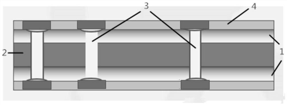
[0038] S2. The outer layer adopts the newly designed negative film engineering data, and dry film 4 is pasted on both sides of the board surface, such as figure 1 As shown, and double-sided exposure, the exposure data is negative polarity;

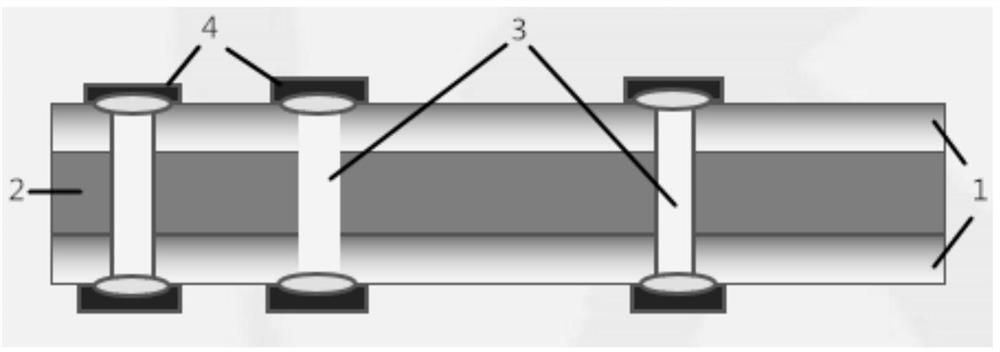
[0039] S3. After standing still for ≥15min, develop. After development, the outer layer is scanned by AOI, and it is confirmed that the dry film 4 completely covers the position of the resin plug hole 3, such as figure 2 shown;

[0040] S4. According to the engineering MI instructions, reduce copper on the plate on the micro-etching line, and u...

Embodiment 2

[0050] A processing technology for micro-etching of resin plug holes in a dry film cover, comprising the following steps:

[0051] S1. Get the engineering data, open the window directly on the resin plug hole 3 of the outer layer cover, the size of the window is 6.5mil larger than the hole diameter on one side, and the alignment system uses a 2.0mm through hole as the alignment reference point;

[0052] S2. The outer layer adopts the newly designed negative film engineering data, and dry film 4 is pasted on both sides of the board surface, such as figure 1 As shown, and double-sided exposure, the exposure data is negative polarity;

[0053] S3. After standing still for ≥15min, develop. After development, the outer layer is scanned by AOI, and it is confirmed that the dry film 4 completely covers the position of the resin plug hole 3, such as figure 2 shown;

[0054] S4. According to the engineering MI instructions, reduce copper on the plate on the micro-etching line, and use...

Embodiment 3

[0064] A processing technology for micro-etching of resin plug holes in a dry film cover, comprising the following steps:

[0065] S1. Get the engineering data, open the window directly on the resin plug hole 3 of the outer layer cover, the size of the window is 6.5mil larger than the hole diameter on one side, and the alignment system uses a 2.0mm through hole as the alignment reference point;

[0066] S2. The outer layer adopts the newly designed negative film engineering data, and dry film 4 is pasted on both sides of the board surface, such as figure 1 As shown, and double-sided exposure, the exposure data is negative polarity;

[0067] S3. After standing still for ≥15min, develop. After development, the outer layer is scanned by AOI, and it is confirmed that the dry film 4 completely covers the position of the resin plug hole 3, such as figure 2 shown;

[0068] S4. According to the engineering MI instructions, reduce copper on the plate on the micro-etching line, and u...


PUM

PropertyMeasurementUnit
thicknessaaaaaaaaaa
thicknessaaaaaaaaaa

Abstract

The invention relates to the technical field of circuit board processing, in particular to a dry film cover resin plug hole micro-etching processing technology. The technology comprises the following steps: directly windowing on a graphic resin plug hole, pasting films on two sides of a board surface, exposing the two sides of the board surface, performing copper reduction on a board at a micro-etching line after determining that a dry film completely covers the position of the resin plug hole, determining that the resin hole plugging position is not corroded, after the plate surface is ground to be flat, developing an outer layer by adopting data of small-size line width/line spacing, a positive film and double-sided exposure data, and after determining that the line width, the line spacing, the BGA, the IC and the MI are consistent, turning to the next process for production. According to the method, hole copper of the resin plug hole can be effectively prevented from being etched in the micro-etching copper reduction process by covering the hole covering dry film on the resin plug hole, the hole opening quality is good, the requirement for manufacturing a circuit board with small line width/line distance can be met, and the effect is good.

Description

technical field [0001] The invention relates to the technical field of circuit board processing, in particular to a processing technology for micro-etching of resin plug holes of a dry film cover. Background technique [0002] With the continuous miniaturization and portability of many electronic products, the functions of electronic products are increasing again and again, which makes the size of PCB in electronic products smaller and smaller, the wiring density is getting denser and the line width of high-precision difficult boards is getting smaller and smaller, Resin plug holes + high copper thickness cannot meet the requirements for etching 3 / 3mil line width and line spacing, and direct micro-etching will cause quality risks to the openings where the resin plug holes are not full, such as uneven openings, lack of copper at the openings, etc. question. [0003] In the early stage, the inventor produced circuit boards with a line width / space of 3 / 3 mil without a micro-et...

Claims


Application Information

Patent Timeline
Patent Type & Authority Applications(China)
IPC IPC(8): H05K3/00H05K3/06
CPCH05K3/0094H05K3/00H05K3/06
Inventor 时兵蔡志浩杨东强黄银燕
Owner 江西志浩电子科技有限公司
Why Eureka
Try Eureka