
Infrared detector pixel and infrared detector based on CMOS process

An infrared detector and pixel technology, applied in the field of infrared detection, can solve the problems of low infrared detector performance, low pixel scale, and low yield rate, and achieve the effects of high detection sensitivity, small chip area, and high yield rate

Active Publication Date: 2021-11-30
BEIJING NORTH GAOYE TECH CO LTD
View PDF8 Cites 0 Cited by
  • Summary
  • Abstract
  • Description
  • Claims
  • Application Information

AI Technical Summary

Problems solved by technology

[0011] In order to solve the above-mentioned technical problems or at least partly solve the above-mentioned technical problems, the present disclosure provides an infrared detector pixel and an infrared detector based on a CMOS process, which solves the problem of low performance and low pixel scale of traditional MEMS process infrared detectors. Problems such as low yield rate, while improving probing performance

Method used


Image

  • Infrared detector pixel and infrared detector based on CMOS process
  • Infrared detector pixel and infrared detector based on CMOS process
  • Infrared detector pixel and infrared detector based on CMOS process

Examples


Embodiment Construction

[0058] To be more clearly understood from the above-mentioned object, features and advantages of the present disclosure, the following disclosure of the present embodiment will be further described. Incidentally, in the case of no conflict, the embodiments of the present disclosure and features in the embodiment may be combined with each other.

[0059] Set forth in the following description, numerous specific details in order to provide a thorough understanding of the present disclosure, the present disclosure also in other ways than described embodiments may be employed; Obviously, the embodiments described in the present disclosure only part of an embodiment, and not all embodiments.

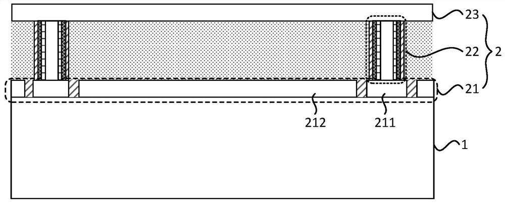
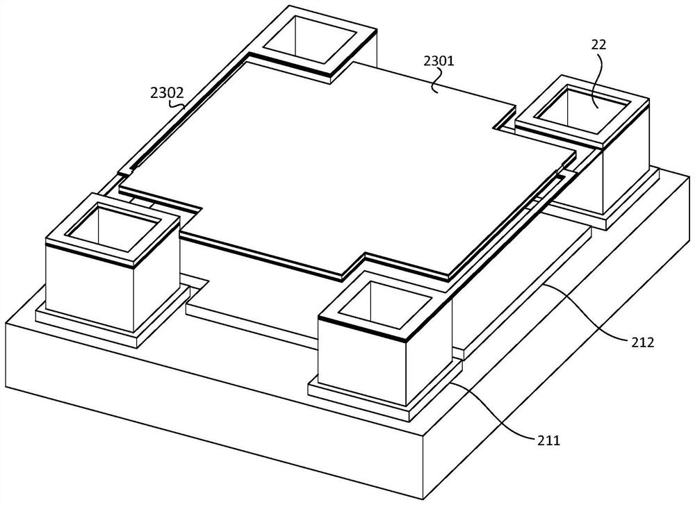
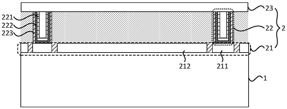
[0060] figure 1 An infrared detector of the present embodiment of the disclosed embodiment as a schematic cross-sectional structure of the element, figure 2 An infrared detector of the present embodiment of the disclosed embodiment as a schematic three-dimensional structure element. Refer figure...


PUM

PropertyMeasurementUnit
Widthaaaaaaaaaa

Abstract

The invention relates to an infrared detector pixel and an infrared detector based on a CMOS process, the pixel comprises a CMOS measurement circuit system and a CMOS infrared sensing structure located on the CMOS measurement circuit system, and the CMOS measurement circuit system and the CMOS infrared sensing structure are prepared by adopting the CMOS process; the CMOS infrared sensing structure comprises a reflecting layer, an infrared conversion structure and a plurality of columnar structures which are located on the CMOS measurement circuit system, the columnar structures are located between the reflecting layer and the infrared conversion structure, the reflecting layer comprises a reflecting plate and a supporting base, and the infrared conversion structure is electrically connected with the CMOS measurement circuit system through the columnar structures and the supporting base; the columnar structures adopt a hollow column, and the side wall of the hollow column is formed by combining metal and a medium. According to the technical scheme, the problems that a traditional MEMS process infrared detector is low in performance, low in pixel scale, low in yield and the like are solved; and the columnar structures adopt the hollow column so that the heat conduction is smaller, the influence of heat radiation generated by the columnar structure on an electric signal of the infrared conversion structure is reduced, and the detection performance is favorably improved.

Description

Technical field [0001] The present disclosure relates to the field of infrared detection, and more particularly to an infrared detector cell and an infrared detector based on a CMOS process. Background technique [0002] Monitor the market, car assistance market, home market, intelligent manufacturing market, and mobile applications have strong demand for non-refrigerated high-performance chips, and the performance of chip performance, consistency, and product price have certain The requirements are expected to have a potential demand for hundreds of millions of chips per year, and the current process programs and architectures cannot meet market demand. [0003] At present, the infrared detector uses the combination of measuring circuits and infrared sensing structures, and the measuring circuit is prepared by CMOS (Complementary Metal-Oxide-Semiconductor, complementary metal oxide semiconductor) process, and the infrared sensing structure uses MEMS (Micro-Electro -Mechanical sy...

Claims


Application Information

Patent Timeline
IPC IPC(8): G01J5/24
CPCG01J5/24G01J2005/0077G01J2005/202Y02P70/50
Inventor 翟光杰武佩潘辉翟光强
Owner BEIJING NORTH GAOYE TECH CO LTD
Learn More