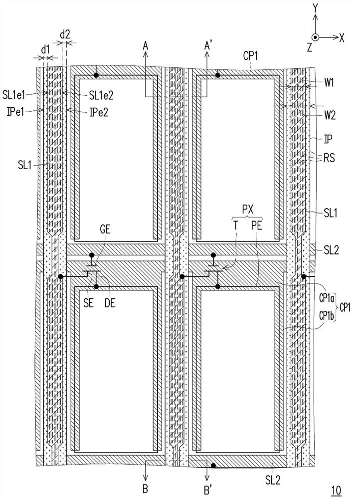
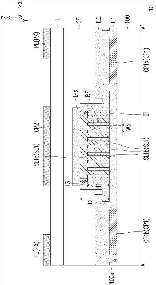
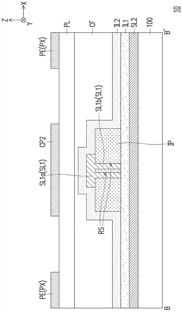
Pixel array substrate
A pixel array substrate and substrate technology, which is applied in instruments, semiconductor devices, optics, etc., can solve problems such as substrate fragmentation, process or optical design limitations, losses, etc., to suppress capacitive coupling effects, improve charge and discharge capabilities, and reduce overall resistance. value effect
- Summary
- Abstract
- Description
- Claims
- Application Information
AI Technical Summary
Problems solved by technology
Method used
Image
Examples
Embodiment Construction
[0046] As used herein, "about," "approximately," "essentially," or "essentially" includes the stated value and the average within an acceptable range of deviation from the particular value as determined by one of ordinary skill in the art, taking into account the The measurement in question and the specific amount of error associated with the measurement (ie, limitations of the measurement system). For example, "about" can mean within one or more standard deviations of the stated value, or for example within ±30%, ±20%, ±15%, ±10%, ±5%. Furthermore, "about", "approximately", "essentially" or "substantially" used herein may select a more acceptable range of deviation or standard deviation according to measurement properties, cutting properties or other properties, and may not use One standard deviation applies to all properties.
[0047] In the drawings, the thickness of layers, films, panels, regions, etc., are exaggerated for clarity. It will be understood that when an elem...
PUM
 Abstract
Description
Claims
Application Information


