Supercharge Your Innovation With Domain-Expert AI Agents!

Vertical structure LED chip and manufacturing method thereof

A LED chip and vertical structure technology, applied in the direction of electrical components, circuits, semiconductor devices, etc., can solve problems such as the complexity of the LED chip manufacturing process, achieve current distribution and expansion performance improvement, excellent light transmittance, and reduce process difficulty. Effect

Pending Publication Date: 2021-12-03
XIAMEN SILAN ADVANCED COMPOUND SEMICON CO LTD
View PDF6 Cites 1 Cited by
  • Summary
  • Abstract
  • Description
  • Claims
  • Application Information

AI Technical Summary

Problems solved by technology

However, LED chips with a vertical positive polarity structure need to use the same-side metal layer scheme, which requires the design and preparation of a complex metal-dielectric-metal stacked layer scheme, and because there must be stress between the metal and the dielectric, during the manufacturing process Especially in the process of bonding and substrate transfer, stress regulation will face greater technical challenges, that is, the manufacturing process of LED chips with vertical positive polarity structure is complicated

Method used


Image

  • Vertical structure LED chip and manufacturing method thereof
  • Vertical structure LED chip and manufacturing method thereof
  • Vertical structure LED chip and manufacturing method thereof

Examples


Embodiment Construction

[0078] Various embodiments of the invention will be described in more detail below with reference to the accompanying drawings. In the various drawings, the same elements are denoted by the same or similar reference numerals. For the sake of clarity, various parts in the drawings have not been drawn to scale.

[0079] The invention can be embodied in various forms, some examples of which are described below.

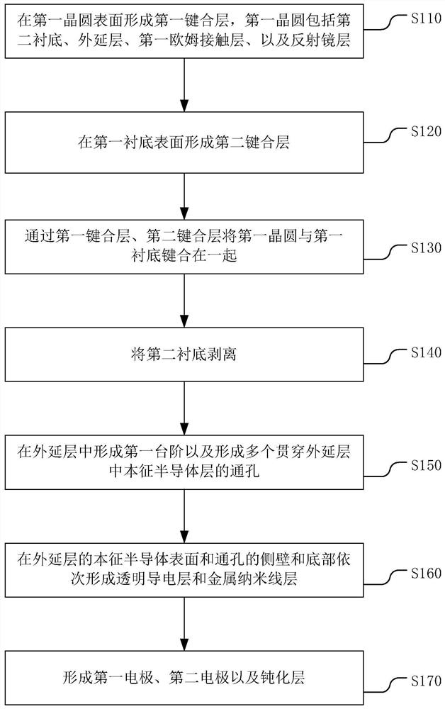
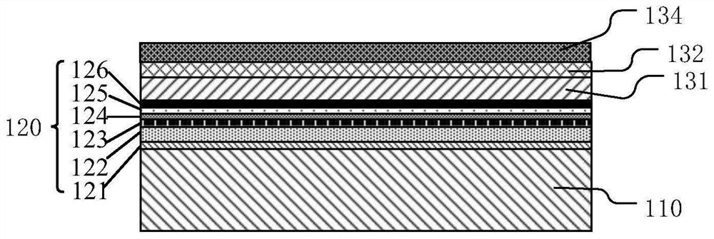
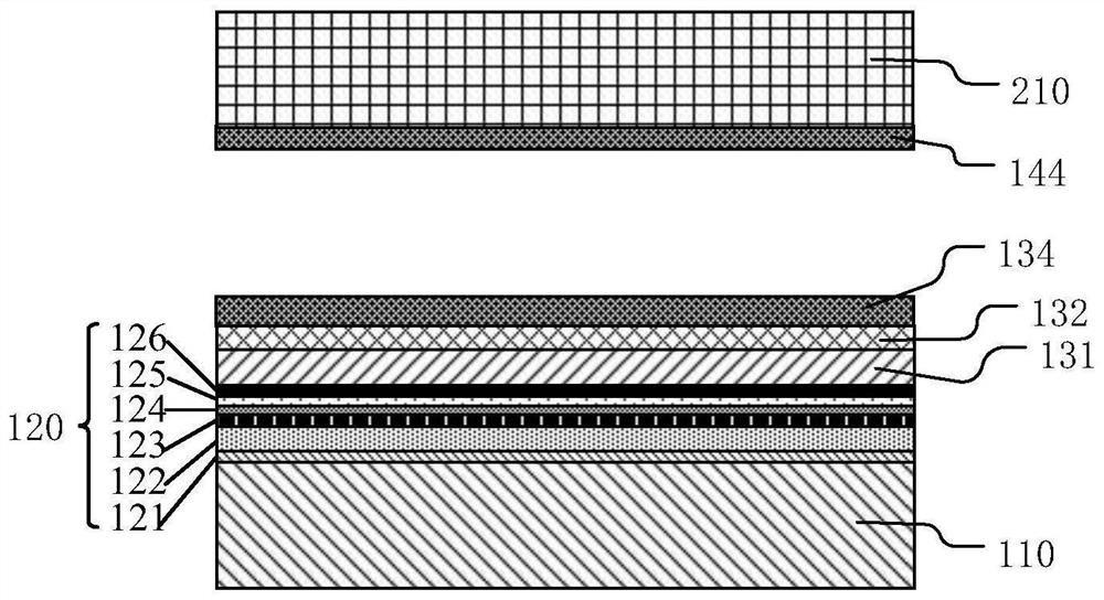
[0080] figure 1 A schematic flowchart of a method for manufacturing a vertical structure LED chip according to an embodiment of the present invention is shown. Figures 2a to 2g The structural cross-sectional views of different stages in the manufacturing process of the vertical structure LED chip provided according to the embodiment of the present invention are shown. image 3 show Figure 2e A top view of the semiconductor structure shown. The manufacturing method provided in this embodiment operates on the entire wafer. For the convenience of understanding, the d...


PUM

PropertyMeasurementUnit
Diameteraaaaaaaaaa
Thicknessaaaaaaaaaa
Thicknessaaaaaaaaaa

Abstract

The invention discloses a vertical structure LED chip and a manufacturing method thereof. The vertical structure LED chip comprises a first substrate, a bonding layer, a reflector layer, a first ohmic contact layer and an epitaxial layer, a plurality of through holes, a transparent conducting layer and a metal nanowire layer, wherein the bonding layer, the reflector layer, the first ohmic contact layer and the epitaxial layerare located on the first surface of the first substrate and are sequentially stacked from bottom to top, the epitaxial layer comprises a second semiconductor layer, a light emitting layer, a first semiconductor layer and an intrinsic semiconductor layer which are located on the surface of the first ohmic contact layer and are sequentially stacked from bottom to top, the through holes penetrate through the intrinsic semiconductor layer and extend out of the surface of the first semiconductor layer, and the transparent conducting layer and the metal nanowire layer are located on the surface of the intrinsic semiconductor layer and the bottoms of the side walls of the through holes. According to the vertical structure LED chip and the manufacturing method thereof of the invention, the surface of the intrinsic semiconductor layer and the side walls and bottoms of the plurality of through holes are provided with the transparent conducting layer and the metal nanowire layer with the resistivity lower than that of the intrinsic semiconductor layer, so that the uniformity of current injection is improved, and a better current expansion effect is obtained.

Description

technical field [0001] The invention belongs to the technical field of semiconductor devices, and more specifically relates to a vertical structure LED chip and a manufacturing method thereof. Background technique [0002] The vertical structure LED chip has the advantage of high brightness compared with the horizontal structure LED chip. On the one hand, the vertical structure LED chip transfers the epitaxial layer from the sapphire substrate with poor insulation and heat dissipation to the bonding substrate with excellent electrical and thermal conductivity, which can withstand higher operating current and obtain higher brightness. On the other hand, the vertical structure LED chip is easier to micro-nano process the light-emitting surface, thereby reducing the total reflection of the epitaxial layer and the air interface to increase the light extraction efficiency. At present, vertical structure LED chips mainly include vertical reverse polarity (N electrode upward) stru...

Claims


Application Information

Patent Timeline
IPC IPC(8): H01L33/38H01L33/14H01L33/06H01L33/46
CPCH01L33/382H01L33/14H01L33/06H01L33/46
Inventor 范伟宏毕京锋郭茂峰李士涛赵进超金全鑫
Owner XIAMEN SILAN ADVANCED COMPOUND SEMICON CO LTD
Features
  • R&D
  • Intellectual Property
  • Life Sciences
  • Materials
  • Tech Scout
  • Unparalleled Data Quality
  • Higher Quality Content
  • 60% Fewer Hallucinations
Learn More