Supercharge Your Innovation With Domain-Expert AI Agents!

Light emitting diode chip and method for manufacturing same

A light-emitting diode and chip technology, applied in electrical components, electrical solid devices, circuits, etc., can solve problems such as high working voltage, high contact resistance of metal electrode layers, and high requirements for uniform distribution, so as to reduce working voltage and improve current distribution Situation, effect of improving heat transfer performance

Active Publication Date: 2013-10-23
APT ELECTRONICS
View PDF0 Cites 0 Cited by
  • Summary
  • Abstract
  • Description
  • Claims
  • Application Information

AI Technical Summary

Problems solved by technology

Although the manufacturing process of the metal electrode layer on the gallium nitride epitaxial wafer has been widely used in silicon integrated circuit technology, for high-power LEDs, due to the large input current, the device requires a uniform distribution of current on the metal electrode layer. Therefore, there are still the following defects at present: First, the structure and design of the existing metal electrode layer cannot provide good current and voltage performance for high-power flip-chip LED devices, resulting in large contact resistance of the metal electrode layer of the device , the working voltage is too high

Method used


Image

  • Light emitting diode chip and method for manufacturing same
  • Light emitting diode chip and method for manufacturing same
  • Light emitting diode chip and method for manufacturing same

Examples


Embodiment Construction

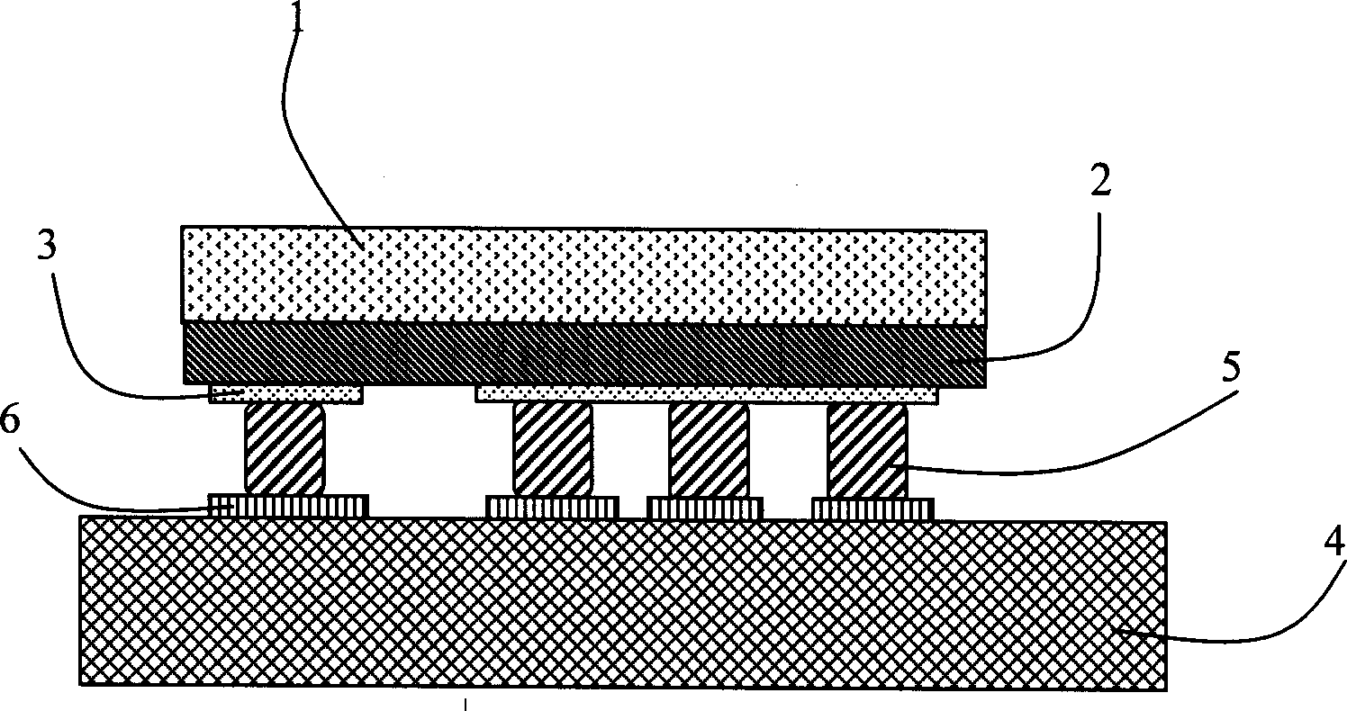
[0038] In this embodiment, a GaN-based epitaxial wafer grown on a transparent aluminum oxide single crystal (ie, a sapphire substrate Sapphire) is used to prepare LED chips for flip-chip bonding. The process is as follows Figure 3a to 3c As shown, the LED chip and its manufacturing process in this embodiment are now specifically described as follows:

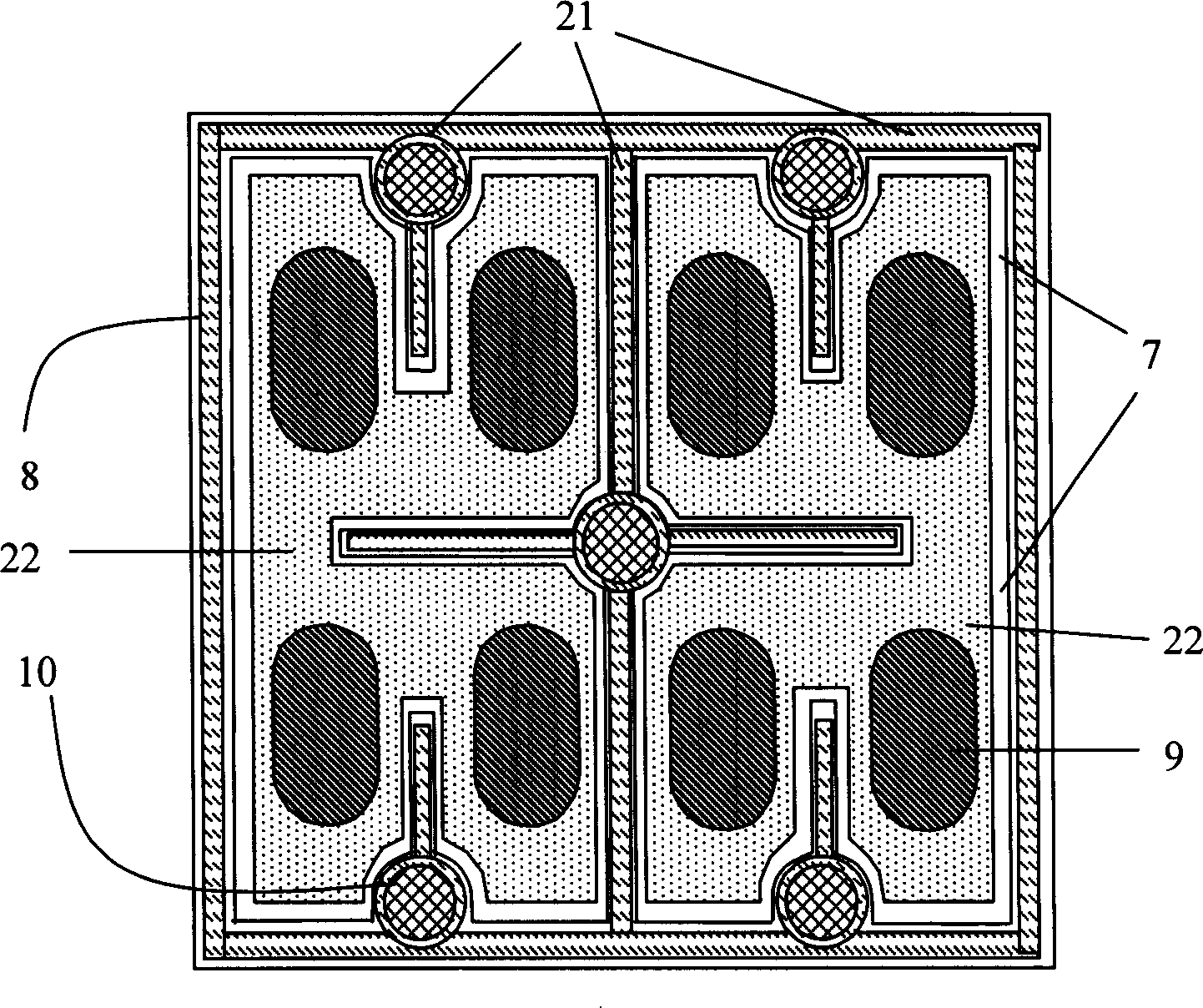
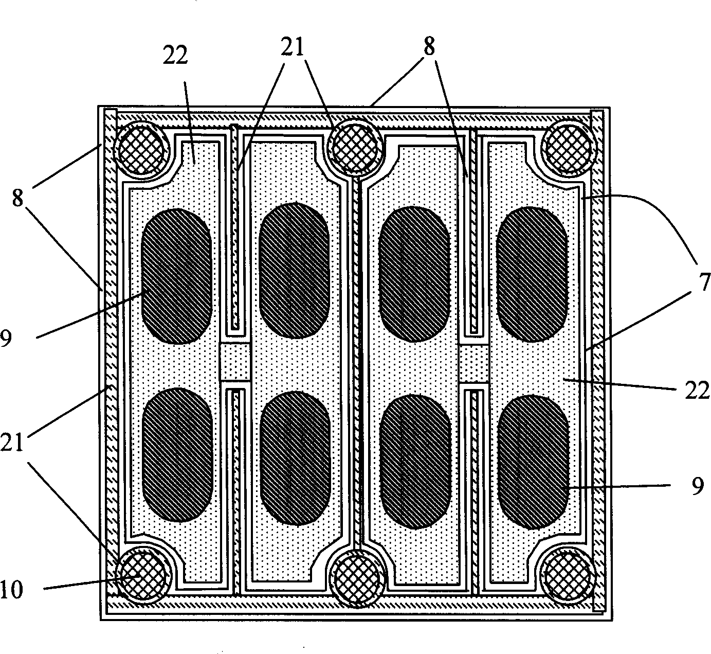
[0039] First, grow a GaN epitaxial wafer on a sapphire substrate 1. According to the design pattern and size of the P-type and N-type regions, an etching process is used to form the P-type region 7 and the N-type region 8 required by the design. Figure 3a Shown. Those skilled in the art can understand that the design graphics conforming to the concept of the present invention can have many variations, for example, Figure 2a to 2g Seven graphic designs conforming to the inventive concept are shown in. The photolithography mask in the etching process can be made according to relevant parameters and design patterns.

[0040] Next, de...


PUM


Abstract

The invention discloses a light emitting diode chip and making method thereof, wherein, the chip comprises an external spreading wafer which is formed on a sapphire substrate, an N type zone and a P type zone of the external spreading wafer are covered with a metal electrode layer which comprises a transparent metal layer and a reflection layer and has a metal layer under convex points and metal convex points; a soleplate for flip chip which is provided with a metal line layer and convex points formed on the metal line layer; wherein, the N type zone surrounds the P type zone as large as possible, and the N type zone is communicated with the metal electrode layer covered on the N type zone and P type zone is divided into a plurality of zones by the N type zone and the metal electrode layer. The metal convex points of the P type zone are evenly distributed on a plurality of divided zones. The invention improves the current distribution conditions by optimized design for device electrode so as to improve the performance and life-span of devices. In addition, the flip chip joint point strength on the electrode and thermal conductivity performance of the device are further improved.

Description

Technical field [0001] The invention relates to a structure design of a light emitting diode (LED) chip and a manufacturing method thereof, in particular to a structure design of a light emitting diode chip with a high-power flip-chip structure and a manufacturing method thereof. Background technique [0002] The electrode metal surface of the traditional light-emitting diode LED die is placed and fixed on a bottom plate. Using wire-bonding technology, the gold wire is welded on the electrode metal layer of the die and connected to the bottom plate. In order to improve current distribution and device performance, on the traditional light-emitting diode die, the positive and negative electrode metal layers cover the entire device, and wire-bonding pads are prepared on this electrode layer for gold wire bonding. Since the light emitting layer of the light emitting diode is below the electrode metal layer, part of the emitted light is absorbed by the electrode metal layer, and this...

Claims


Application Information

Patent Timeline
Patent Type & Authority Patents(China)
IPC IPC(8): H01L33/00H01L33/36H01L33/62
CPCH01L2224/11H01L2224/16225
Inventor 肖国伟陈正豪
Owner APT ELECTRONICS
Features
  • R&D
  • Intellectual Property
  • Life Sciences
  • Materials
  • Tech Scout
  • Unparalleled Data Quality
  • Higher Quality Content
  • 60% Fewer Hallucinations
Learn More