Low quiescent current NMOS type fully-integrated LDO circuit
A quiescent current, fully integrated technology, applied in the direction of adjusting electrical variables, control/regulating systems, instruments, etc., can solve the problems of unexpected circuit restart, increase of LDO quiescent current, large LDO overshoot, etc., to improve PSRR and reduce static electricity. Current, the effect of speeding up recovery
- Summary
- Abstract
- Description
- Claims
- Application Information
AI Technical Summary
Problems solved by technology
Method used
Image

Examples
Embodiment
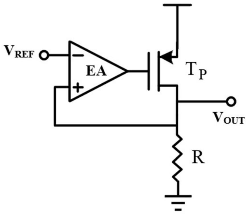
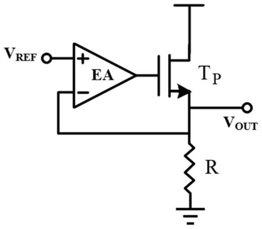
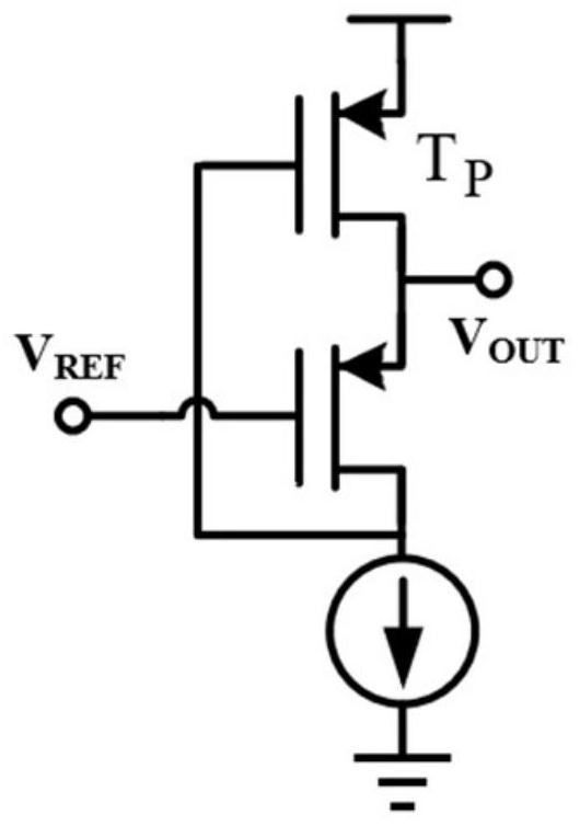
[0066] see Figure 4 As shown, the present invention provides a low quiescent current NMOS type fully integrated LDO circuit, including an error amplifier circuit, an adaptive bias current source circuit, an NMOS transistor N5 as a power transmission tube, resistors R1 and R2 as load resistors, and a frequency A compensation circuit, an upper overshoot detection circuit and a lower overshoot detection circuit, the upper overshoot detection circuit adaptively controls the opening and closing of the NMOS transistor N6, and the lower overshoot detection circuit adaptively controls the opening and closing of the PMOS transistor P5 ;
[0067] The overshoot detection circuit is configured to turn on the NMOS transistor N6 when detecting the occurrence of the overshoot, so as to provide an additional bias current to the error amplifier circuit, and turn off the NMOS when the output overshoot voltage returns to a value close to the steady state Tube N6;
[0068] The undershoot detec...
Embodiment approach
[0104] The embodiment of the present invention is realized under the 180nm CMOS process, and the goal is to provide the core with a power supply voltage of 1.2V and a maximum load current of 50mA. The operating voltage of the error amplifier circuit may be 2.5-5V, and the power supply voltage of the NMOS transistor N5 may be 1.25-1.6V. The no-load quiescent current of the present invention is only 3.6 μA, realizing the goal of low quiescent current.
[0105] The advantages of the present invention are specifically described below in conjunction with the accompanying drawings
[0106] see Figure 7 As shown, when the load current is switched between 200 μA and 50 mA in 1 ns, the present invention has the effect of obviously accelerating the overshoot recovery speed, and the increase of the lower overshoot recovery speed is particularly obvious.
[0107] see Figure 8 As shown, the undershoot voltage can be restored to within 10% of the final value (ie 1.15V) within 160ns.
...
PUM
 Abstract
Description
Claims
Application Information
 - R&D
- Intellectual Property
- Life Sciences
- Materials
- Tech Scout
- Unparalleled Data Quality
- Higher Quality Content
- 60% Fewer Hallucinations
Browse by: Latest US Patents, China's latest patents, Technical Efficacy Thesaurus, Application Domain, Technology Topic, Popular Technical Reports.
© 2025 PatSnap. All rights reserved.Legal|Privacy policy|Modern Slavery Act Transparency Statement|Sitemap|About US| Contact US: help@patsnap.com