SOI wafer with high heat dissipation performance and preparation method of SOI wafer

A high heat dissipation, wafer technology, applied in semiconductor/solid-state device manufacturing, electrical components, electric solid-state devices, etc., can solve the problem of low thermal conductivity of buried oxide layer, device channel current drop, application limitations of semiconductor-on-insulator technology, etc. problem, to achieve the effect of improving utilization rate, increasing integration, and improving heat dissipation performance

Active Publication Date: 2021-12-07
MICROTERA SEMICON (GUANGZHOU) CO LTD
View PDF7 Cites 6 Cited by
  • Summary
  • Abstract
  • Description
  • Claims
  • Application Information

AI Technical Summary

Problems solved by technology

However, due to the relatively low thermal conductivity of the buried oxide layer, there is a self-heating effect in the high-density integrated SOI circuit, resulting in a decrease in the channel current of the device and the formation of negative differential resistance, which greatly limits the application of semiconductor-on-insulator technology. limit

Method used


Image

  • SOI wafer with high heat dissipation performance and preparation method of SOI wafer
  • SOI wafer with high heat dissipation performance and preparation method of SOI wafer
  • SOI wafer with high heat dissipation performance and preparation method of SOI wafer

Examples


Embodiment Construction

[0026] Embodiments of the present invention are described below through specific examples, and those skilled in the art can easily understand other advantages and effects of the present invention from the content disclosed in this specification. The present invention can also be implemented or applied through other different specific implementation modes, and various modifications or changes can be made to the details in this specification based on different viewpoints and applications without departing from the spirit of the present invention.

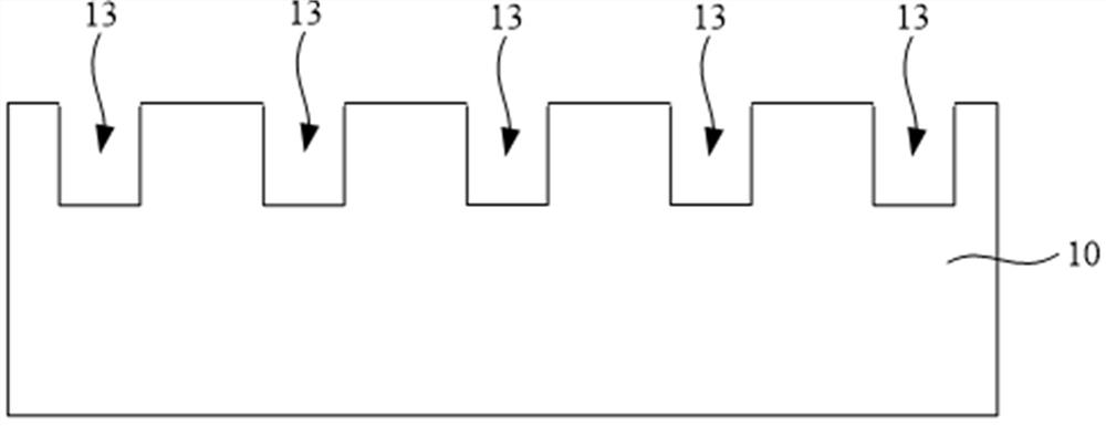
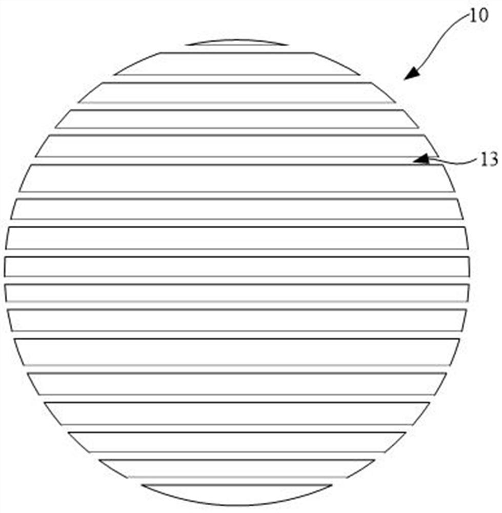
[0027] For example, when describing the embodiments of the present invention in detail, for the convenience of explanation, the cross-sectional view showing the device structure will not be partially enlarged according to the general scale, and the schematic diagram is only an example, which should not limit the protection scope of the present invention. In addition, the three-dimensional space dimensions of length, width and depth sho...


PUM


Abstract

The invention provides an SOI wafer with high heat dissipation performance and a preparation method of the SOI wafer. The SOI wafer sequentially comprises a bulk silicon wafer, a buried oxide layer and a silicon device layer, a groove with a preset depth is formed in one side, close to the buried oxide layer, of the bulk silicon wafer, the groove is filled with a high-thermal-conductivity material, the high-thermal-conductivity material is fixed by adopting heat dissipation glue, and the high-thermal-conductivity material is a carbon nano tube or molybdenum disulfide. According to the invention, the grooves are formed in the bulk silicon wafer, and the grooves are filled with the high-thermal-conductivity material made of the carbon nanotubes or the molybdenum disulfide, so that the heat dissipation performance of an SOI circuit can be effectively improved based on the high thermal conductivity of the carbon nanotubes and the molybdenum disulfide, and the size of the SOI wafer is made to be larger; in addition, the high-thermal-conductivity material is arranged in the bulk silicon wafer, the area of the silicon device layer is not affected, the utilization rate of the active region is improved, the cost is reduced, and the integration level is improved.

Description

technical field [0001] The invention relates to the technical field of semiconductor-on-insulator substrates, in particular to an SOI wafer with high heat dissipation performance and a preparation method thereof. Background technique [0002] Due to the advantages of low parasitic junction capacitance and Buried Oxid (BOX) isolation, Silicon-on-Insulator (SOI) technology is widely used in low-power, high-speed and high-reliability integrated circuits. However, due to the relatively low thermal conductivity of the buried oxide layer, there is a self-heating effect in the high-density integrated SOI circuit, resulting in a decrease in the channel current of the device and the formation of negative differential resistance, which greatly limits the application of semiconductor-on-insulator technology. limit. [0003] Therefore, it is necessary to propose an SOI wafer with high heat dissipation performance and a preparation method thereof, so as to effectively improve the heat d...

Claims


Application Information

Patent Timeline
Patent Type & Authority Applications(China)
IPC IPC(8): H01L23/367H01L27/12H01L23/373H01L21/762
CPCH01L23/367H01L27/1203H01L23/373H01L21/7624
Inventor 刘森刘海彬关宇轩刘兴龙班桂春
Owner MICROTERA SEMICON (GUANGZHOU) CO LTD
Why Eureka
Try Eureka