Supercharge Your Innovation With Domain-Expert AI Agents!

SiC LDMOS device and manufacturing method thereof

A manufacturing method and device technology, applied in semiconductor/solid-state device manufacturing, semiconductor devices, electrical components, etc., can solve problems such as poor performance and low switching frequency, and achieve the effect of eliminating Cgd, small Cgd, and improving switching frequency and performance.

Active Publication Date: 2021-12-10
SHENZHEN BASIC SEMICON LTD
View PDF4 Cites 0 Cited by
  • Summary
  • Abstract
  • Description
  • Claims
  • Application Information

AI Technical Summary

Problems solved by technology

[0005] This application provides a SiC LDMOS device and its manufacturing method, aiming to solve the problems of low switching frequency and poor performance of LDMOS devices in the related art

Method used


Image

  • SiC LDMOS device and manufacturing method thereof
  • SiC LDMOS device and manufacturing method thereof
  • SiC LDMOS device and manufacturing method thereof

Examples


Embodiment Construction

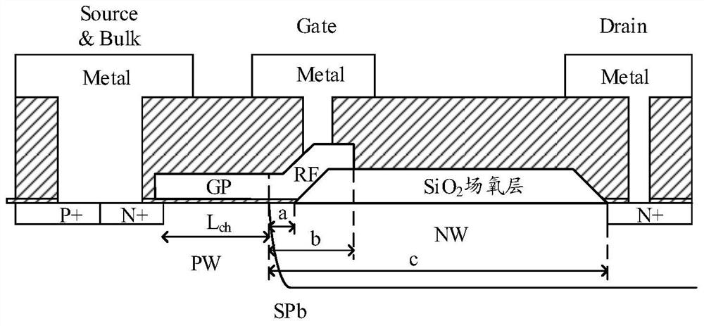
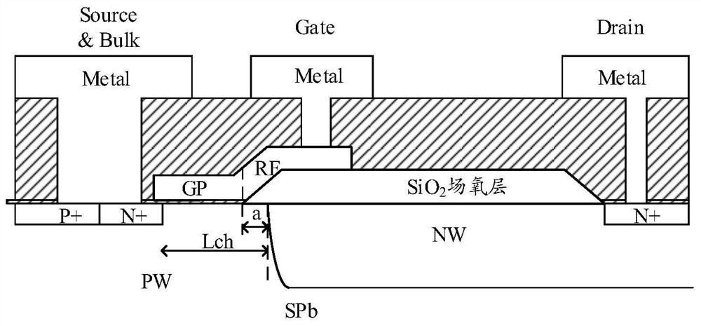
[0046] In order to make the purpose, technical solutions and advantages of the application more obvious and understandable, the following will clearly and completely describe the application in conjunction with the embodiments of the application and the corresponding drawings, wherein the same or similar symbols throughout represent the same or similar elements or elements having the same or similar functions. It should be understood that the various embodiments of the application described below are only used to explain the application, and are not intended to limit the application, that is, based on the various embodiments of the application, those skilled in the art will not make an inventive step. All other embodiments obtained under the premise of labor all belong to the protection scope of this application. In addition, the technical features involved in the various embodiments of the present application described below may be combined with each other as long as they do ...


PUM


Abstract

The invention provides a SiC LDMOS device and a manufacturing method thereof. The SiC LDMOS device comprises a SiC substrate, a P well region, an N well region, a source region P+, a source region N+, a drain region N+, a gate oxide layer, a polysilicon gate and a SiN field oxide layer, wherein the SiN field oxide layer covers the surface, corresponding to the N well region, of the SiC substrate, the edge, close to the source region N+, of the SiN field oxide layer is aligned with the edge, close to the source region N+, of the N well region, and the side, close to the drain region N+, of the SiN field oxide layer is provided with an inclined plane. The edge, close to the drain region N+, of the SiN field oxide layer is aligned with the edge, close to the source region N+, of the drain region N+, the surface, not covered with the SiN field oxide layer, of the SiC substrate is covered with the gate oxide layer, the surface, corresponding to the P well region, of the gate oxide layer is covered with the polysilicon gate, and the edge, close to the drain region N+, of the polysilicon gate is connected with the edge, close to the source region N+, of the SiN field oxide layer. And one side, far away from the drain region N+, of the polysilicon gate is overlapped with one side, close to the drain region N+, of the source region N+. Smaller Cgd can be realized, even the Cgd can be completely eliminated, so that the switching frequency and the performance of the LDMOS device can be effectively improved.

Description

【Technical field】 [0001] The present application relates to the technical field of power electronic devices, in particular to a SiC LDMOS device and a manufacturing method thereof. 【Background technique】 [0002] In related technologies, since the characteristic indicators of SiC (Silicon Carbide, silicon carbide) such as bandgap width, critical breakdown electric field, thermal conductivity and carrier saturation drift velocity are more than three times that of Si (Silicon, silicon), so SiC It has become an excellent material for making power electronic devices, such as making LDMOS (Laterally Double-Diffused Metal-Oxide-Semiconductor, laterally double-diffused metal-oxide-semiconductor) devices and MOSFET (Metal-Oxide-Semiconductor Field-Effect Transistor , metal-oxide-semiconductor field-effect transistor) devices, etc. Compared with MOSFET devices, LDMOS devices have the advantages of high gain, wide linear range and small distortion; moreover, the Source (source region...

Claims


Application Information

Patent Timeline
IPC IPC(8): H01L29/78H01L29/40H01L21/04
CPCH01L29/7816H01L29/402H01L21/0445H01L29/66068
Inventor 杜蕾和巍巍汪之涵喻双柏张振中
Owner SHENZHEN BASIC SEMICON LTD
Features
  • R&D
  • Intellectual Property
  • Life Sciences
  • Materials
  • Tech Scout
  • Unparalleled Data Quality
  • Higher Quality Content
  • 60% Fewer Hallucinations
Learn More