Supercharge Your Innovation With Domain-Expert AI Agents!

Supporting an optical element

A technology of optical components and components, applied in the direction of optical components, optics, optomechanical equipment, etc., can solve the problem of uneven distribution of impact load

Pending Publication Date: 2021-12-17
CARL ZEISS SMT GMBH
View PDF2 Cites 0 Cited by
  • Summary
  • Abstract
  • Description
  • Claims
  • Application Information

AI Technical Summary

Problems solved by technology

So, in this case also the shock load on the individual holding units is not evenly distributed; rather, most of the shock load has to be absorbed by several individual holding devices
Furthermore, a problem that naturally arises due to this statically overdetermined support is that parasitic stresses in the case of deformation of the support ring are introduced into the optical element

Method used


Image

  • Supporting an optical element
  • Supporting an optical element
  • Supporting an optical element

Examples


no. 1 example

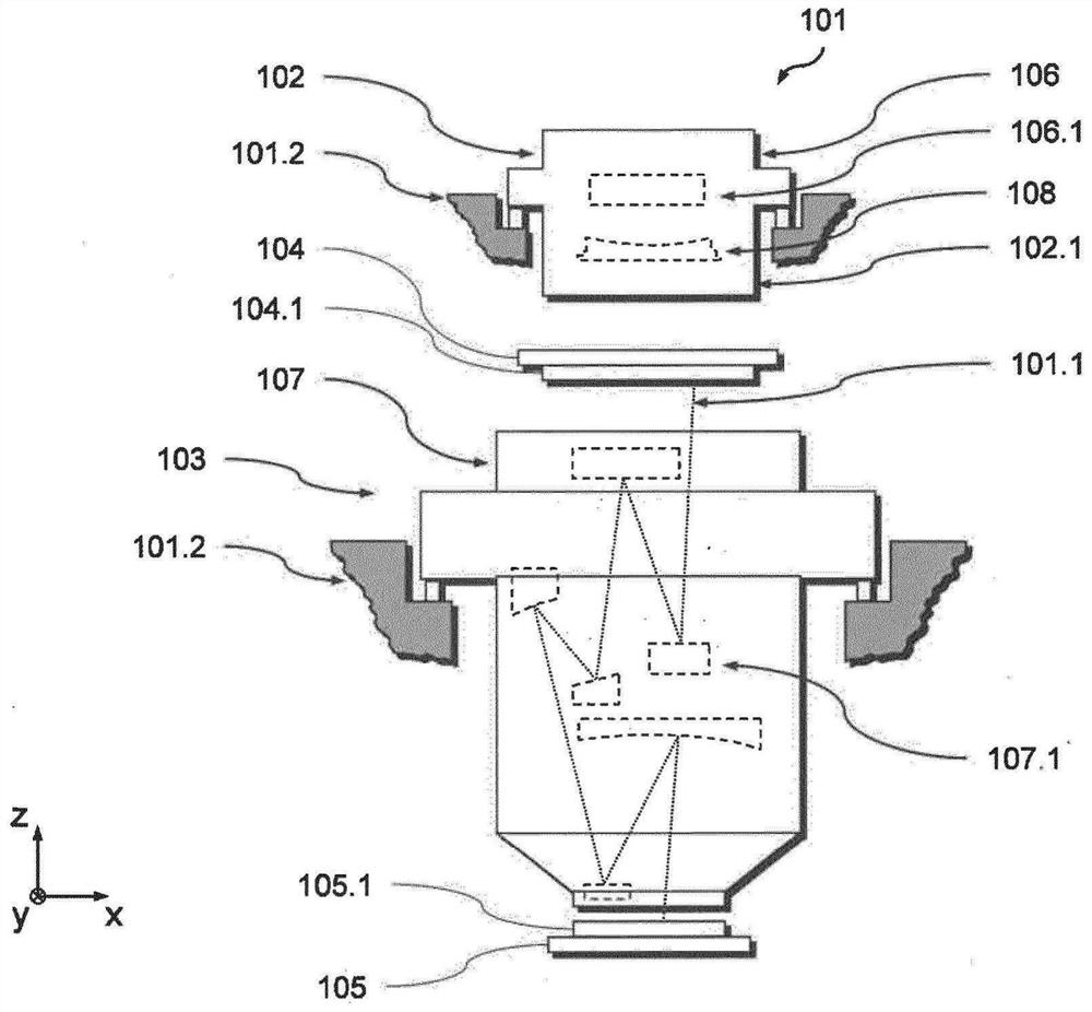
[0090] The following reference Figure 1 to Figure 4 A preferred embodiment of a microlithographic projection exposure apparatus 101 according to the invention is described, comprising a preferred embodiment of the optical arrangement according to the invention. To simplify the following explanations, an x, y, z coordinate system is indicated in the attached drawings, the z direction corresponding to the direction of gravity. It goes without saying that any desired other orientation of the x, y, z coordinate system can be selected in a further configuration.

[0091] figure 1 is a schematic, not to scale representation of a projection exposure apparatus 101 used in a microlithography process for producing semiconductor components. The projection exposure apparatus 101 comprises an illumination device 102 and a projection device 103 . The projection device 103 is designed to transfer an image of the structure of the mask 104.1 arranged in the mask unit 104 onto the substrate...

no. 2 example

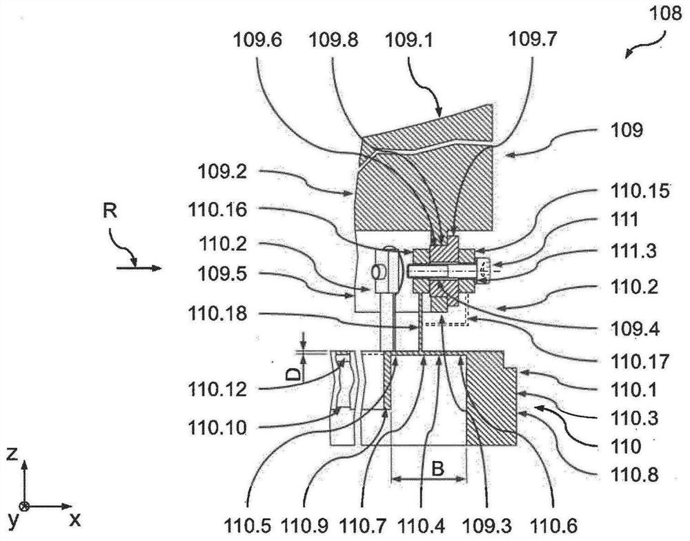
[0163] The following reference figure 1 , figure 2 ,and Figure 5 to Figure 7 A further preferred embodiment of the arrangement 208 according to the invention which can be used instead of the arrangement 108 in the imaging device 101 is illustrated. Arrangement 208 corresponds in its basic design and function to that from Figure 2 to Figure 4 108, so only the differences will be discussed here. In particular, identical parts are provided with identical reference numerals, whereas similar parts are provided with reference numerals incremented by the value 100. Unless stated otherwise below, reference is made to the above statements in relation to the first embodiment as to the features, functions, and advantages of these components.


PUM


Abstract

The present invention relates to an arrangement of a microlithographic imaging device, particularly for using light in the extreme UV (EUV) range, comprising a holding device (110) for holding an optical element (109), wherein the optical element (109) comprises an optical surface (109.1) and defines a plane of main extension, in which the optical element (109) defines a radial direction and a circumferential direction. The holding device (110) comprises a base unit (110.1) and more than three separate holding units (110.2), wherein the base unit (110.1) comprises a plurality of support interface units (110.3), which are spaced apart from one another in the circumferential direction, for connecting the holding device (110) to a support structure (102.1). The holding units (110.2) are connected to the base unit (110.1) and disposed in a manner distributed along the circumferential direction and spaced apart from one another. The holding units (110.2) are configured to hold the optical element (109) with respect to the base unit (110.1 ). The base unit comprises at least one support membrane element (110.4), wherein the at least one support membrane element (110.4) predominantly extends along the circumferential direction and along the radial direction, wherein the at least one support membrane element (110.4) has a thickness dimension transversely to the circumferential direction and radial direction. The holding units (110.2) are disposed on a front side of the at least one support membrane element (110.4) that faces the optical element (109).

Description

[0001] Cross References to Related Applications [0002] This application claims priority under 35 U.S.C. §119 to German Patent Application No. 102019 112224.4 filed May 10, 2019, the entire contents of which are incorporated herein by reference. technical field [0003] The present invention relates to an optical arrangement for microlithography suitable for use with UV imaging light, in particular light in the extreme ultraviolet (EUV) range. Furthermore, the invention relates to an optical imaging device comprising such an arrangement. The present invention can be used with any desired optical imaging method. In particular it can be advantageously used in the production or inspection of microelectronic circuits and optical components for this purpose (eg optical masks). Background technique [0004] Optical devices used in the production of microelectronic circuits usually include a plurality of optical element units, which include one or more optical elements, such as ...

Claims


Application Information

Patent Timeline
IPC IPC(8): G03F7/20G02B7/02G02B7/182G02B7/00G02B27/64
CPCG03F7/7015G03F7/70825G02B7/026G02B7/182G02B7/00G02B27/646G02B7/02
Inventor C.科尔纳C.米勒E.安塞尔姆
Owner CARL ZEISS SMT GMBH
Features
  • R&D
  • Intellectual Property
  • Life Sciences
  • Materials
  • Tech Scout
  • Unparalleled Data Quality
  • Higher Quality Content
  • 60% Fewer Hallucinations
Learn More