
Automatic glue coating and spinning device for semiconductor silicon wafer and key structure of automatic glue coating and spinning device

A technology for semiconductors and silicon wafers, which is applied to the field of automatic gluing and gluing devices for semiconductor silicon wafers, can solve problems such as inability to meet the requirements of use and small motor torque, and achieve the effects of simple structure, prevention of air leakage and novel design.

Pending Publication Date: 2021-12-21
MAXONE SEMICON CO LTD
View PDF0 Cites 1 Cited by
  • Summary
  • Abstract
  • Description
  • Claims
  • Application Information

AI Technical Summary

Problems solved by technology

[0003] At present, there are many problems in the process of using the automatic glue coating and rejection device for semiconductor silicon wafers, such as the high speed, high torque, and vacuum adsorption compatibility of large-size silicon wafers. The classic method of silicon wafer adsorption and rejection is that the vacuum air circuit passes through the motor. The bottom, the hollow shaft of the motor, the silicon wafer suction cup, and the silicon wafer are connected together. The silicon wafer is firmly adsorbed on the silicon wafer suction cup by vacuum suction, and then the motor rotates at a high speed to drive the silicon wafer to rotate and apply glue; the silicon wafer size ( 8 inches, diameter 200mm), high speed (5000r / min), according to the torque calculation formula, it can be seen that the starting torque to drive the silicon wafer to rotate at high speed is 0.3N m, plus the safety factor, friction, etc., the required motor torque is 0.8 More than N m, the domestic conventional hollow motor can reach the speed, but the motor torque is very small (0.1 N m); the motor torque can meet the requirements, but the motor shaft is a solid shaft, and the rated speed is 3000r / min, which cannot Meet the use

Method used


Image

  • Automatic glue coating and spinning device for semiconductor silicon wafer and key structure of automatic glue coating and spinning device
  • Automatic glue coating and spinning device for semiconductor silicon wafer and key structure of automatic glue coating and spinning device
  • Automatic glue coating and spinning device for semiconductor silicon wafer and key structure of automatic glue coating and spinning device

Examples


specific Embodiment 1

[0040] The following example is an embodiment of the automatic coating device of a semiconductor wafer according to the present application.

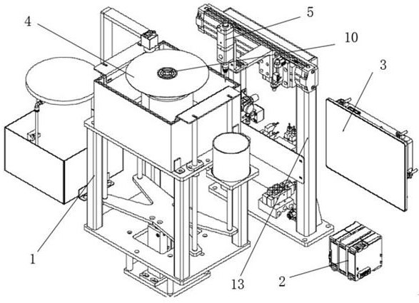
[0041] See Figure 1-12 As shown, a semiconductor silicon wafer automatic coating rubber device includes a body 1, a mounting frame 13, a PLC2, a manual interface 3, a rubber assembly 4, a flash assembly 5, and a high speed vacuum assembly 10; wherein the body One side is fixedly connected to the mounting frame 13, the top side of the mounting frame 13 is fixedly connected to the drip assembly 5, and the bottom side of the drip assembly 5 is provided with a rubber assembly 4 placed in the body 1, the spin glue. A high speed vacuum assembly 10 is provided in the assembly 4, and the human machine interface 3 and PLC2 provided on one side of the body 1;

[0042] The rubber assembly 4 includes a lifting cylinder 406, a lifting plate 405, a silicon wafer 401, a gelatin thickness sensor 402, a guide post 403, and a connecting frame 404, and the li...

specific Embodiment 2

[0054] The following example is an embodiment of a gelatin assembly according to a semiconductor wafer automatic coating rubber device, which can be performed separately, and can be automatically applied as a semiconductor wafer disclosed in the specific embodiment. Key structure of glue rubber device.

[0055] A gelatin assembly of a semiconductor wafer automatic coating rubber rubber device, including: lifting cylinder 406, a lift plate 405, a silicon wafer 401, a glue thickness sensor 402, a guide post 403, and a connecting frame 404, the lifting cylinder 406 fixed Connecting on the bottom side of the body 1, the lift cylinder 406 is fixedly coupled with a lifting plate 405, and the top side of the lifting plate 405 is fixedly coupled with a guide post 403, and the tip of the guide post 403 is fixedly connected to the lifting cover 15, said The lifting cover 15 outer wall slid on the cover 16, the shroud 16 is provided with a base 14 fixed to the top side of the body 1, and the...

specific Embodiment 3

[0057] The following example is an example of a drip assembly of a semiconductor wafer automatic coating glue apparatus, which can be carried out alone and can be automatically applied as a semiconductor wafer disclosed in the specific embodiment. Key structure of glue rubber device.

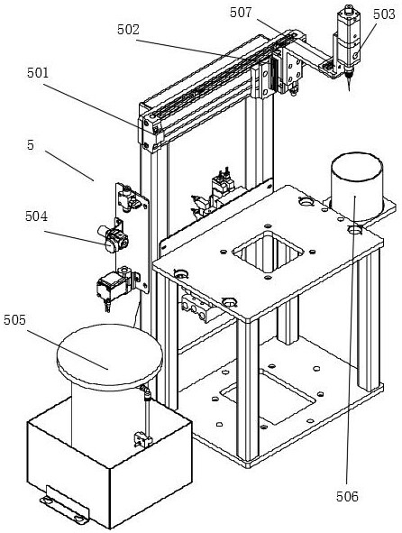
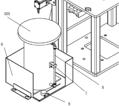
[0058] A semiconductor silicon wafer automatic coating glue apparatus of a glue device, including: horizontal cylinder 501, vertical cylinder 502, drip valve 503, pressure regulator valve 504, colloidal pressure can 505, a raised container 506, and a fixing frame 507, The horizontal cylinder 501 is fixedly coupled to the top side surface of the mounting frame 13, the horizontal cylinder 501 output, and the vertical cylinder 502 is fixed, and the vertical cylinder 502 is fixedly connected to the fixing frame 507, the fixing frame 507 side. The surface is fixedly connected with a drip valve 503, and the drip valve 503 is provided with a regulator valve 504 on the communication gas path of the colloida...


PUM


Abstract

The invention discloses an automatic glue coating and spinning device for a semiconductor silicon wafer and a key structure of the automatic glue coating and spinning device. The automatic glue coating and spinning device comprises a machine body, a mounting frame, a PLC, a human-computer interface, a glue spinning assembly, a glue dripping assembly and a high-speed vacuum suction assembly, wherein the mounting frame is fixedly connected to one side of the machine body, the glue dripping assembly is fixedly connected to the top side of the mounting frame, the glue spinning assembly is arranged on the bottom side of the glue dripping assembly, the high-speed vacuum suction assembly is arranged in the glue rotating assembly, the glue spinning assembly comprises a lifting air cylinder, a lifting plate, a silicon wafer, a glue thickness measuring sensor, a guide column and a connecting frame, the glue dripping assembly comprises a horizontal air cylinder, a vertical air cylinder, a glue dripping valve, a pressure regulating valve, a glue pressure tank, a glue discharging container and a fixing frame, and the high-speed vacuum suction assembly comprises a suction cup, a high-speed cyclone component, a speed increaser and a motor. The automatic glue coating and spinning device for the semiconductor silicon wafer is novel in design and simple in structure, meets the requirement of high rotating speed through the small-torque motor, and can ensure that the silicon wafer is stably connected at the high rotating speed.

Description

Technical field [0001] The present invention relates to a semiconductor wafer automatic coating rubber device and a key structure thereof, belonging to the semiconductor wafer automatic coating glue application technology. Background technique [0002] During the semiconductor chip lithographic production process, the silicon wafer needs to be surface cleaning, cast, spin coated photoresist, soft baking, cooling, etc., the spin coated photoresist is an important part; in the spin In the coated gel, there are two process methods; one is static coating, i.e. silicon is stationary, drip, accelerated rotation, glue, volatile solvent; the other is dynamic rubber, ie low speed rotation (500R) / min), drip, accelerated rotation (5000R / min), glue, volatile solvent : The viscosity of the photoresist, the lower the viscosity, the thinner thickness of the photoresist; the speed of rotation, the speed is, the thickness is thin; the speed of rotation, the faster the acceleration, the more u...

Claims


Application Information

Patent Timeline
Patent Type & Authority Applications(China)
IPC IPC(8): G03F7/16B05C13/02B05C11/08B05C5/02
CPCG03F7/162B05C5/0225B05C11/08B05C13/02B05C5/02
Inventor 于海超徐兴光
Owner MAXONE SEMICON CO LTD
Learn More