Cutting method and silicon wafer
A cutting method and slicing technology, applied in stone processing equipment, photovoltaic power generation, electrical components, etc., can solve problems such as tension fluctuations and high wire breakage rates
- Summary
- Abstract
- Description
- Claims
- Application Information
AI Technical Summary
Problems solved by technology
Method used
Image

Examples
Embodiment Construction
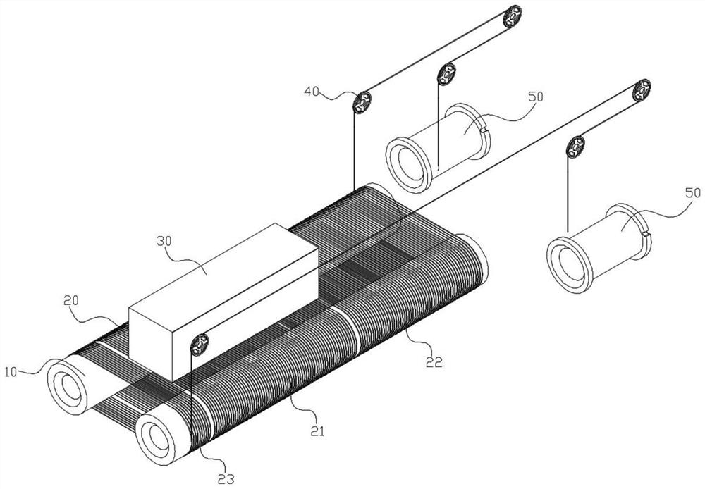
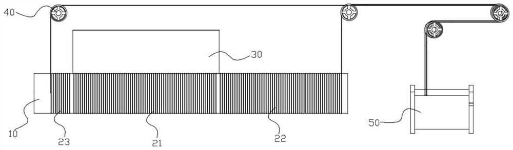
[0026] In order to clearly describe the technical solutions of the embodiments of the present invention, in the embodiments of the present invention, words such as "first" and "second" are used to distinguish the same or similar items with basically the same function and effect. Those skilled in the art can understand that words such as "first" and "second" do not limit the number and execution order, and words such as "first" and "second" do not necessarily limit the difference.
[0027] In the description of the present invention, it should be understood that the orientation or positional relationship indicated by the terms "upper", "lower", "front", "rear", "left", "right" etc. are based on those shown in the accompanying drawings. Orientation or positional relationship is only for the convenience of describing the present invention and simplifying the description, and does not indicate or imply that the referred device or element must have a specific orientation, be constru...
PUM
| Property | Measurement | Unit |
|---|---|---|
| diameter | aaaaa | aaaaa |
| thickness | aaaaa | aaaaa |
Abstract
Description
Claims
Application Information