
High electron mobility transistor and high voltage semiconductor device

A high electron mobility, transistor technology, used in semiconductor devices, circuits, electrical components, etc., can solve problems such as reducing breakdown voltage and reliability, leakage current, and increasing semiconductor device off-current, avoiding on-resistance, reducing The effect of cutting off the current and improving the distribution of the surface electric field

Pending Publication Date: 2021-12-31
VANGUARD INTERNATIONAL SEMICONDUCTOR CORPORATION
View PDF0 Cites 0 Cited by
  • Summary
  • Abstract
  • Description
  • Claims
  • Application Information

AI Technical Summary

Problems solved by technology

However, during the process of forming an ohmic contact, the metal in the drain electrode usually reacts with the underlying semiconductor layer to form spiking defects, so that the local electric field adjacent to the spiking defects will be large, causing unnecessary Leakage current phenomenon, thereby increasing the cut-off current (I OFF ), reduce breakdown voltage and reliability

Method used


Image

  • High electron mobility transistor and high voltage semiconductor device
  • High electron mobility transistor and high voltage semiconductor device
  • High electron mobility transistor and high voltage semiconductor device

Examples


Embodiment Construction

[0030] The invention provides a number of different embodiments that can be used to implement the different features of the invention. Examples of specific components and arrangements are also described herein for simplicity of description. These examples are provided for the purpose of illustration only, without any limitation. For example, the following description of "the first feature is formed on or over the second feature" may refer to "the first feature is in direct contact with the second feature" or "the first feature is in direct contact with the second feature". There are other features between the features", so that the first feature is not in direct contact with the second feature. In addition, the various embodiments of the present invention may use repeated reference signs and / or text notations. The use of these repeated reference signs and notations is to make the description more concise and clear, but not to indicate the relationship between different embod...


PUM


Abstract

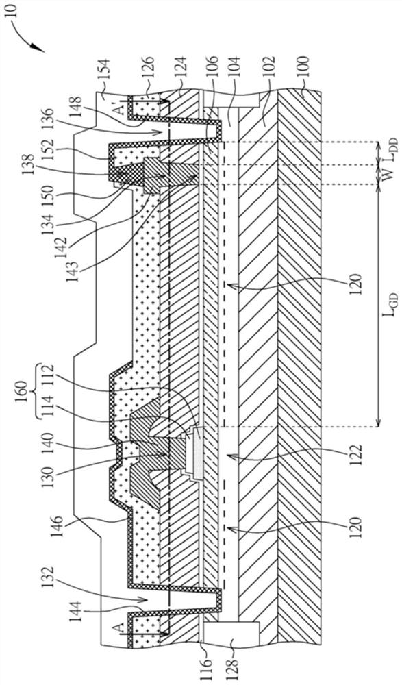
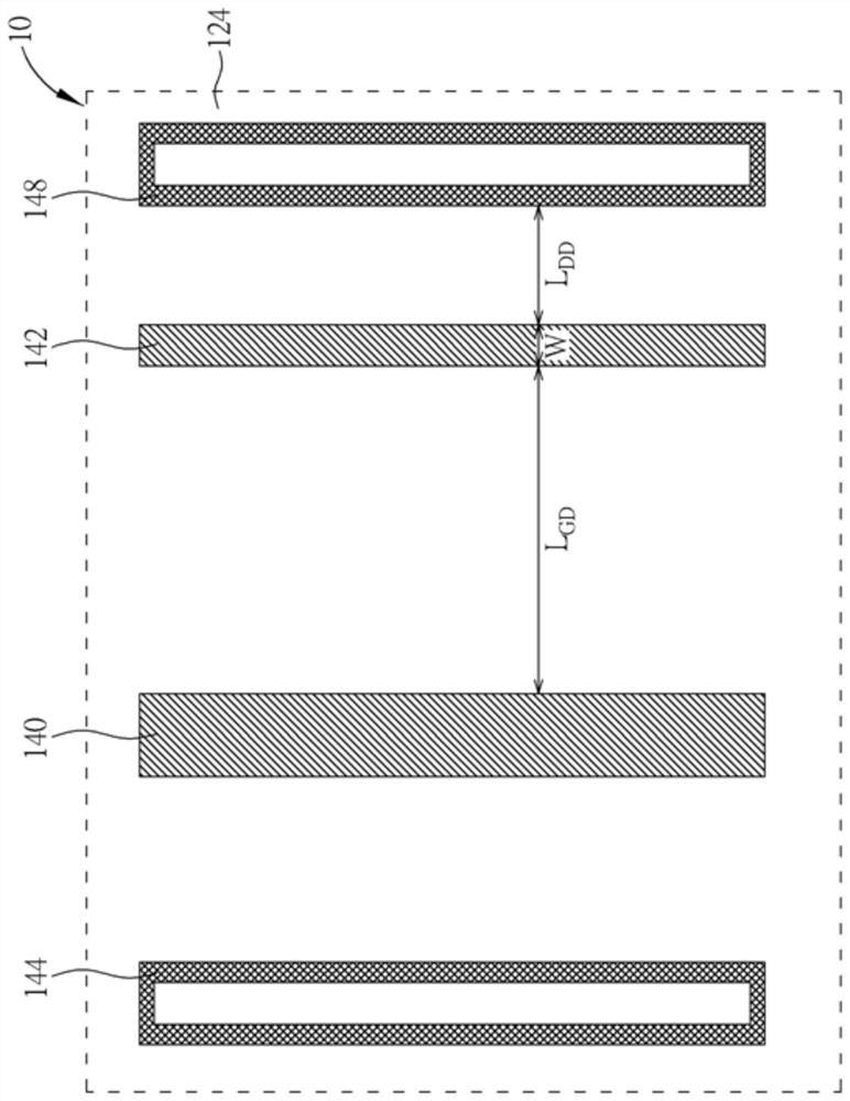
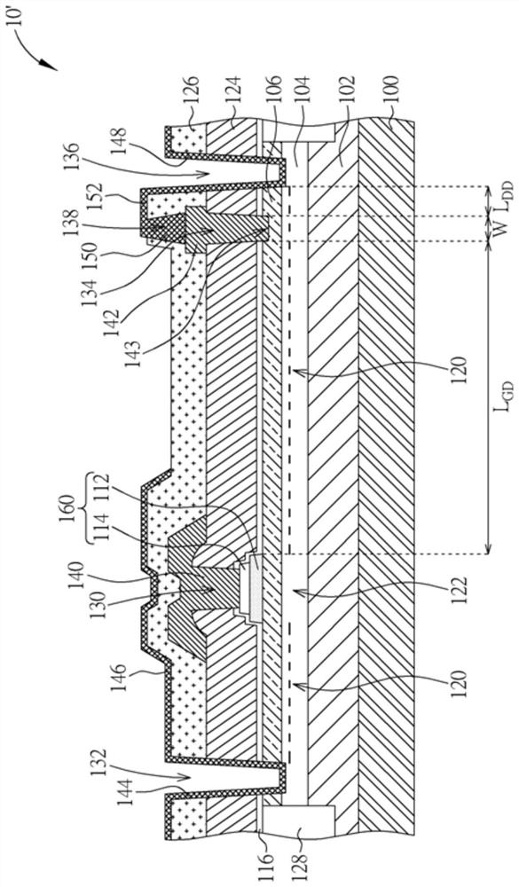
The invention discloses a high electron mobility transistor which includes a substrate, a III-V channel layer, a III-V barrier layer, a III-V cover layer, a source electrode, a first drain electrode, a second drain electrode and a connecting part, wherein the III-V channel layer, the III-V barrier layer and the III-V cover layer are sequentially arranged on the substrate; the source electrode is disposed on one side of the III-V cover layer, and the first drain electrode and the second drain electrode are disposed on the other side of the III-V cover layer; the bottom surface of the first drain electrode is separated from the bottom surface of the second drain electrode, and the composition of the first drain electrode is different from the composition of the second drain electrode; and the connecting part is electrically connected to the first drain electrode and the second drain electrode.

Description

technical field [0001] The invention relates to the field of semiconductor devices, in particular to a high-electron mobility transistor and a high-voltage semiconductor device. Background technique [0002] In semiconductor technology, III-V semiconductor compounds can be used to form various integrated circuit devices, such as high power field effect transistors, high frequency transistors or high electron mobility transistors (high electron mobility transistors, HEMTs). HEMT is a transistor with two-dimensional electron gas (two dimensional electron gas, 2-DEG), and its 2-DEG will be adjacent to the junction between two materials with different energy gaps (that is, the heterogeneous junction ). Since HEMT does not use doped regions as the carrier channel of the transistor, but uses 2-DEG as the carrier channel of the transistor, HEMT has several attractive features compared to the known metal oxide half field effect transistor (MOSFET). properties such as high electron...

Claims


Application Information

Patent Timeline
Patent Type & Authority Applications(China)
IPC IPC(8): H01L29/778H01L29/40H01L29/45H01L29/47H01L29/08
CPCH01L29/7783H01L29/402H01L29/475H01L29/452H01L29/0843
Inventor 黄嘉庆陈志谚吴俊仪萧智仁
Owner VANGUARD INTERNATIONAL SEMICONDUCTOR CORPORATION
Learn More