Hysteresis comparison control circuit
A technology of control circuit and hysteresis comparison, applied in the field of control circuit with hysteresis function, can solve the problems of complicated operation, shortened fan life, self-locking, etc., to achieve stable and reliable operation, low static power consumption, and wide application.
- Summary
- Abstract
- Description
- Claims
- Application Information
AI Technical Summary
Problems solved by technology
Method used
Image

Examples
no. 1 example
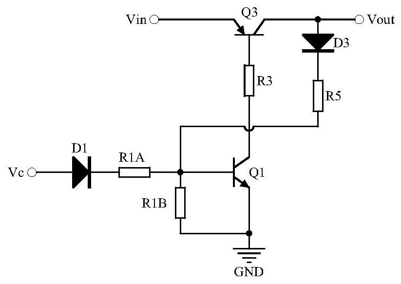
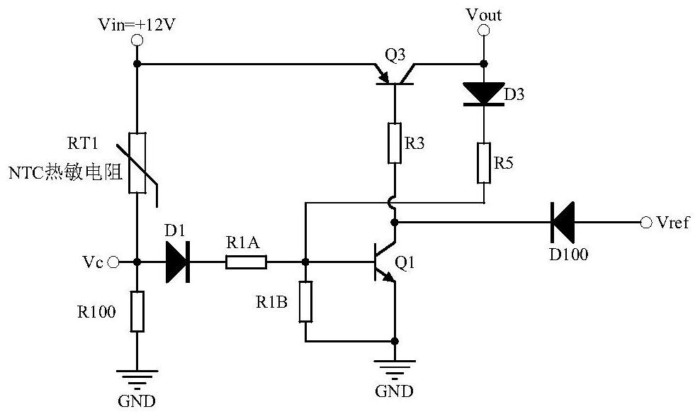
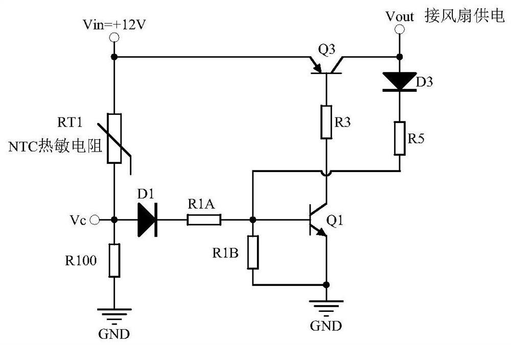
[0078] Such as diagram 2-1 As shown, the schematic circuit diagram of the first embodiment of the present invention includes NPN transistor Q1, NPN transistor Q2, PNP transistor Q3, PNP transistor Q4, diode D1, diode D2, diode D3, resistor R1A, resistor R1B, resistor R2A, resistor R2B, resistor R3, resistor R4, resistor R5.
[0079] The base of transistor Q1 is connected to one end of resistor R1B and the other end of resistor R1A at the same time, one end of resistor R1A is connected to the cathode of diode D1, and the anode of diode D1 is connected to the control signal Vc and the anode of diode D2 at the same time; the other end of resistor R1B is connected to The emitter of the transistor Q1 and the ground terminal GND; the collector of the transistor Q1 is connected to the other end of the resistor R3, one end of the resistor R3 is connected to the base of the transistor Q3, the emitter of the transistor Q3 is connected to the input voltage Vin, and the collector of the ...
no. 2 example
[0095] Such as image 3 As shown, it is the schematic circuit diagram of the second embodiment of the present invention. Compared with the first embodiment of the present invention, the difference of the second embodiment is that it also includes a capacitor C1 and a capacitor C2, and the capacitor C1 is connected across the transistor Q1 Between the base and the emitter of the transistor Q2, the capacitor C2 is connected between the base and the emitter of the transistor Q2.
[0096] After adding capacitors C1 and C2, the high-frequency interference signal at the control signal Vc will be bypassed by capacitors C1 and C2 to ensure that transistors Q1 and Q2 will not be turned on or off by mistake, thereby improving the anti-interference ability of the circuit.
[0097] Compared with the first embodiment of the present invention, the basic working principle of the second embodiment is not substantially different, and will not be repeated here.
no. 3 example
[0099] Such as Pic 4-1 As shown, it is the schematic diagram of the third embodiment of the present invention. Compared with the first embodiment of the present invention, the difference of the third embodiment is that it also includes a resistor R6 and a resistor R7, and one end of the resistor R6 is connected to the transistor Q3. The other end of the resistor R6 is connected to the collector of the transistor Q1; one end of the resistor R7 is connected to the emitter of the transistor Q4, and the other end of the resistor R7 is connected to the collector of the transistor Q2.
[0100] After adding resistors R6 and R7, there is another way for the collector bias current of transistor Q1 and transistor Q2, so that it is more convenient to adjust the working state of transistor Q3 and transistor Q4 (amplification area or saturation area), so that circuit debugging more simple. Compared with the first embodiment of the present invention, the working principle of the third emb...
PUM
 Abstract
Description
Claims
Application Information
 - Generate Ideas
- Intellectual Property
- Life Sciences
- Materials
- Tech Scout
- Unparalleled Data Quality
- Higher Quality Content
- 60% Fewer Hallucinations
Browse by: Latest US Patents, China's latest patents, Technical Efficacy Thesaurus, Application Domain, Technology Topic, Popular Technical Reports.
© 2025 PatSnap. All rights reserved.Legal|Privacy policy|Modern Slavery Act Transparency Statement|Sitemap|About US| Contact US: help@patsnap.com