Interface characteristic measurement method based on electronic Goos-Hanchen shift
A technology of interface characteristics and measurement methods, applied in the direction of measuring devices, semiconductor/solid-state device testing/measurement, circuits, etc., to achieve the effect of easy operation and simple thinking
- Summary
- Abstract
- Description
- Claims
- Application Information
AI Technical Summary
Problems solved by technology
Method used
Image

Examples
Embodiment 1
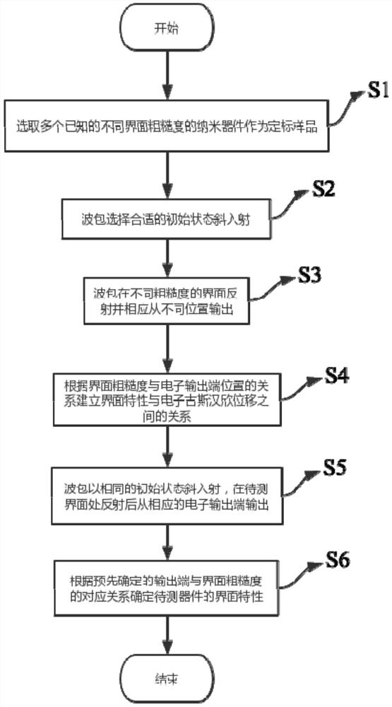
[0076] Embodiment 1: Measuring interface roughness
[0077] When the applicant studied the movement trajectory of the electron beam in the two-dimensional conductive layer, it was found that if a rough interface barrier is formed on the two-dimensional conductive layer, the electron beam is reflected on the rough interface, and the resulting Goos-Hanchen shift will be reduced. , and the Goos-Hanchen shifts of the electron beam after reflection on different rough interfaces are also different. Electron dynamics can be studied by analogy to the optical Gouss-Hanchen shift. Due to the volatility of electrons, when the incident electron beam is emitted to an interface with different potential energy or effective mass, total reflection occurs, and the phase shift of different plane waves is different, and displacement will occur along the interface. The principle of this displacement is similar to that of optical Gus-Hanchen Displacement, that is, the Goos-Hanchen shift of the inc...
Embodiment 2
[0089] Example 2: Measuring the height of the interface barrier
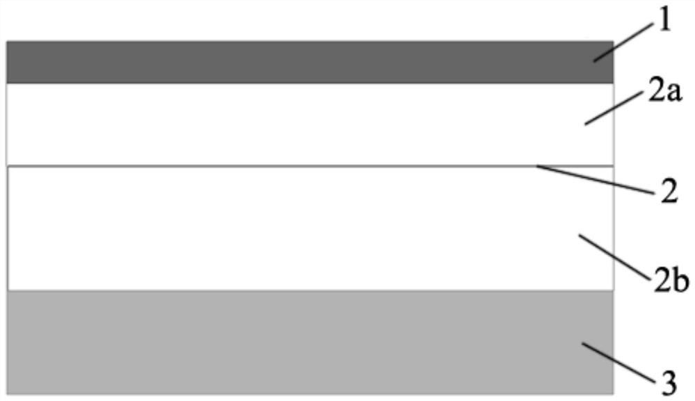
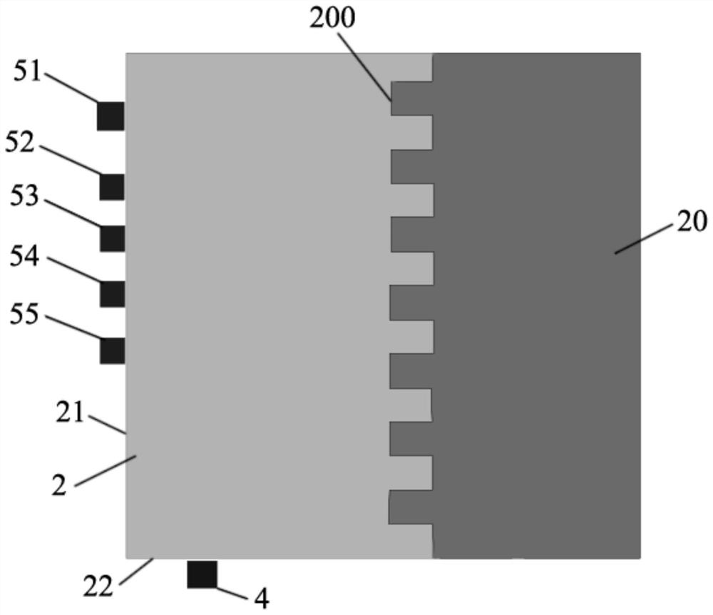
[0090] In this embodiment, experiments are conducted to explore the relationship between the interface barrier height and the electron Goos-Hanchen shift. This example uses figure 2 The measurement setup shown, but where the barrier shape and interface of the two-dimensional conductive layer 2 are the same as image 3 shown differently.
[0091] In the experiment, such as figure 2 As shown, the two-dimensional conductive layer 2 is a two-dimensional electron gas layer formed by the heterojunction interface of the stacked GaAs layer and AlGaAs layer. As shown in Figure 9(a), the two-dimensional conductive layer 2 is a square with a width of 150nm and a length of 150nm; a two-dimensional rectangular potential barrier with a smooth interface on the left side is formed in the two-dimensional electronic layer, and the potential barrier The potential energies are respectively 0.02eV, 0.025eV, 0.03eV, 0.035eV and...
Embodiment 3
[0095] Example 3: Distinguishing the interfaces on both sides of the gradient barrier
[0096] In this embodiment, the relationship between the interface of the linear gradient barrier and the electron Goos-Hanchen shift is explored through experiments. This example uses figure 2 The measurement setup shown, but where the barrier shape and interface of the two-dimensional conductive layer 2 are the same as image 3 shown differently.
[0097] In the experiment, such as figure 2 As shown, the two-dimensional conductive layer 2 is a two-dimensional electron gas layer formed by the heterojunction interface of the stacked GaAs layer and AlGaAs layer. For example, as shown in Figure 10(a) and Figure 10(b), the two-dimensional conductive layer 2 is a square with a width of 150nm and a length of 150nm; the left side of the two-dimensional electronic layer forms a linear gradient with a smooth interface Potential barrier, the width of the potential barrier is 20nm. The X-Y coor...
PUM
| Property | Measurement | Unit |
|---|---|---|
| Width | aaaaa | aaaaa |
| Length | aaaaa | aaaaa |
| Width | aaaaa | aaaaa |
Abstract
Description
Claims
Application Information
 - R&D Engineer
- R&D Manager
- IP Professional
- Industry Leading Data Capabilities
- Powerful AI technology
- Patent DNA Extraction
Browse by: Latest US Patents, China's latest patents, Technical Efficacy Thesaurus, Application Domain, Technology Topic.
© 2024 PatSnap. All rights reserved.Legal|Privacy policy|Modern Slavery Act Transparency Statement|Sitemap