Laser detection system for visually measuring film stress

A thin-film stress, laser detection technology, applied in semiconductor/solid-state device testing/measurement, electrical components, circuits, etc., can solve the problems of cumbersome inspection process and low accuracy, and achieve cumbersome process, high measurement accuracy and maintenance. high cost effect

Pending Publication Date: 2022-01-04
EAST CHINA NORMAL UNIV
View PDF0 Cites 2 Cited by
  • Summary
  • Abstract
  • Description
  • Claims
  • Application Information

AI Technical Summary

Problems solved by technology

[0006] Aiming at the problems of cumbersome detection process and low accuracy of the existing traditional method for detecting the stress change of the thin film, the present invention provides a laser detection system for visually measuring the stress of the thin film, which uses the laser measuring element on the measuring device to measure the edge of the wafer. The curvature radius value of the average distribution point at any angle in the diameter direction to obtain the measurement results more quickly; through the visualization platform, the stress value at any point on the horizontal line at any angle along the diameter direction of the wafer surface after the photoresist film is completely displayed , radius of curvature, and degree of curvature, so that defective chips can be detected more intuitively and quickly

Method used


Image

  • Laser detection system for visually measuring film stress
  • Laser detection system for visually measuring film stress
  • Laser detection system for visually measuring film stress

Examples


Embodiment 1

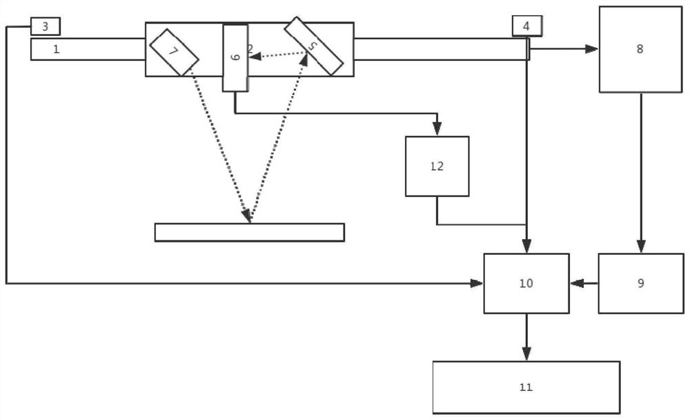
[0062] A visual laser measurement film stress detection system, including:

[0063] A laser measurement module, the laser measurement module at least includes a one-dimensional linear sensor 6, the laser measurement module is configured to emit laser light to the surface of the wafer and irradiate the laser reflected by the wafer onto the one-dimensional linear sensor 6;

[0064] In this embodiment, the laser measurement module is the basis for realizing the measurement of the film stress. In terms of specific design, the laser measurement module includes:

[0065] The laser 7 is used to emit laser light of a certain wavelength and irradiate the surface of the wafer;

[0066] The mirror 5 is used to conduct the laser light reflected from the surface of the wafer;

[0067] Driven by the one-dimensional screw rod carrying platform, the laser 7 passes the center point of the wafer and makes a one-dimensional movement along the diameter of the wafer. After the laser light of a c...

Embodiment 2

[0088] It is basically the same as Example 1. It can be seen from Embodiment 1 that, for the main control terminal, the main control terminal is configured to calculate the stress data of the wafer film according to the current change at both ends of the light curtain on the one-dimensional linear sensor, and generate a visualization based on the stress data of the wafer film Order. Therefore, for the main control terminal, how to calculate the stress data of the wafer film according to the current change at both ends of the light curtain on the one-dimensional linear sensor is a technical problem to be solved urgently in this embodiment. Based on this, further, the main control terminal is configured to calculate the stress data of the wafer film according to the current change at both ends of the light curtain on the one-dimensional linear sensor, including:

[0089] S1. Convert the upper current and lower current at both ends of the upper light curtain of the one-dimension...

Embodiment 3

[0105] It is basically the same as Example 2. In order to know more intuitively the unevenness of the wafer surface and to visualize the unevenness of the wafer surface, we need to know the curvature of the wafer film on each acquisition. Therefore in this embodiment, further, also include:

[0106] According to the stress data of the wafer film, take the center point of the wafer as the warp center, extend the distribution to the left and right of the center point, and establish the distribution relationship of the curvature of the wafer film.

[0107] It specifically includes:

[0108] The distribution relationship of the curvature of the wafer center point to the left is:

[0109] The distribution relationship of the rightward curvature of the wafer center point is:

[0110] In the above formula, B is the curvature of the current point, B i-1 is the curvature of the previous point, and d is the distance between two adjacent points of the collection point on the wafe...


PUM


Abstract

The invention discloses a laser detection system for visually measuring film stress, and belongs to the technical field of semiconductor manufacturing and detection. The system comprises a laser measurement module, the laser measurement module at least comprises a one-dimensional linear sensor, wherein the laser measurement module is configured to emit laser to the surface of a wafer and irradiate the laser reflected by the wafer to the one-dimensional linear sensor; an acquisition end configured to acquire current changes at the two ends of the light curtain on the one-dimensional linear sensor; a main control end, wherein the main control end is in wireless communication connection with the acquisition end, and the main control end is configured to calculate wafer film stress data according to current changes at the two ends of a light curtain on the one-dimensional linear sensor and generate a visual command according to the wafer film stress data, and send the visual data to a visual terminal which is in communication connection with the main control end for real-time display. Data visualization is adopted, different wafer sizes and different coating materials are manually selected for measurement through the visualization platform, and multiple purposes are achieved through one machine.

Description

technical field [0001] The invention belongs to the technical field of semiconductor manufacturing and detection, and more specifically relates to a laser detection system for visually measuring film stress. Background technique [0002] In the entire process of chip manufacturing, semiconductor wafers need to be coated with a photoresist film for light transmission before photolithography. One of the common wafer coating processes is to drop a drop of photoresist on the center of the wafer, and rotate the wafer to spray the photoresist evenly on the surface of the wafer through centrifugal force; the other is to atomize the photoresist spray The method makes the photoresist evenly sprayed on the surface of the wafer. [0003] No matter which method is used to coat the semiconductor wafer, it is necessary to check the film uniformity of the wafer after coating. The film uniformity of the wafer can be measured by measuring the stress value of the wafer film to measure whethe...

Claims


Application Information

Patent Timeline
Patent Type & Authority Applications(China)
IPC IPC(8): H01L21/66
CPCH01L22/12H01L22/24H01L22/20
Inventor 陈闻杰林晓坤王成真牛康宇谢子苗
Owner EAST CHINA NORMAL UNIV
Why Eureka
Try Eureka