Preparation process of high-heat-dissipation multi-layer PCB

A technology of PCB circuit board and preparation process, which is applied in the direction of multilayer circuit manufacturing, printed circuit manufacturing, printed circuit, etc. Problems such as heat accumulation, to achieve the effect of ensuring heat transfer efficiency, improving production safety, and ensuring stability and safety

Pending Publication Date: 2022-01-07
深圳市广诚达电路技术有限公司
View PDF5 Cites 0 Cited by
  • Summary
  • Abstract
  • Description
  • Claims
  • Application Information

AI Technical Summary

Problems solved by technology

[0004] The multi-layer PCB circuit board in the prior art is composed of multiple single-layer circuit boards stacked together, so that the circuits in the unit space are integrated too much, which leads to the internal occurrence of the multi-layer circuit board when it is actually working. The heat is more concentrated, and the heat generated in the inner circuit board is difficult to dissipate quickly, resulting in the accumulation of heat in the multilayer circuit board, which easily affects the working stability of the multilayer circuit board, and even causes dangers such as burning in serious cases. ACCIDENT

Method used


Image

  • Preparation process of high-heat-dissipation multi-layer PCB
  • Preparation process of high-heat-dissipation multi-layer PCB
  • Preparation process of high-heat-dissipation multi-layer PCB

Examples


Embodiment 1

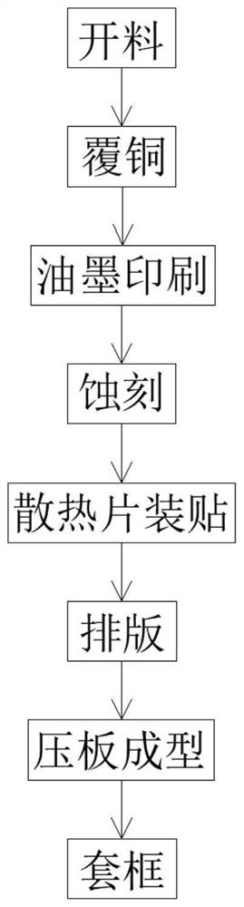
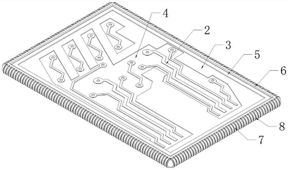
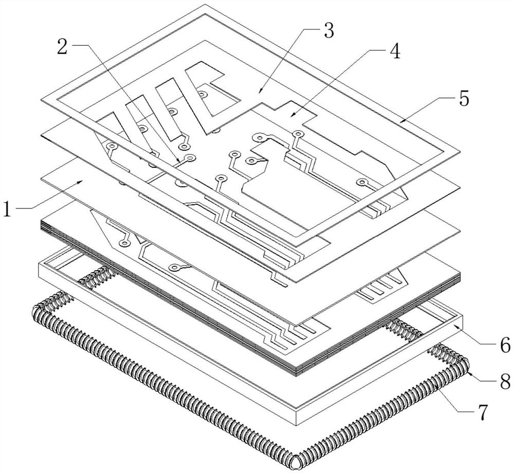
[0053] see Figure 1-10 , a preparation process of a high heat dissipation multilayer PCB circuit board, comprising the following steps:

[0054] S1, material cutting, according to the design requirements of the produced PCB circuit board, the entire PCB board is cut into substrates 1 of equal size by a cutting device;

[0055] S2, copper covering, according to the design requirements of the PCB circuit board, evenly and fixedly cover the metal copper layer on the outer surface of the substrate 1;

[0056] S3, ink printing, printing the pre-designed circuit ink layer on the metal copper layer on the outer surface of the substrate 1 through a hot press;

[0057] S4, etching, the substrate 1 after ink printing is put into the inside of the etching device, and the metal copper layer not covered by the circuit ink layer on the outer surface of the substrate 1 is corroded by the overlooking liquid in the etching device, and the metal under the circuit ink layer is corroded. The c...


PUM


Abstract

The invention discloses a preparation process of a high-heat-dissipation multi-layer PCB, and belongs to the field of PCB preparation. The preparation process of the high-heat-dissipation multi-layer PCB can quickly dissipate accumulated heat in an inner-layer space of the multi-layer PCB, the outer surface of each substrate is covered with a heat dissipation copper plate, silicone grease is brushed in through grooves formed in the heat dissipation copper plates, heat generated when the wire works can be effectively absorbed, and a copper frame wrapping the outer side of the circuit board group is matched, so that the heat transmitted on the heat dissipation copper plates can be quickly diffused outwards, the high heat dissipation performance of the multi-layer PCB is effectively improved, the problem that heat generated when the wire located on the inner-layer substrate works is difficult to dissipate outwards quickly is avoided, and the working stability of the multi-layer PCB produced through the technology is improved conveniently.

Description

technical field [0001] The invention relates to the field of PCB circuit board preparation, and more specifically, relates to a preparation process of a high heat dissipation multilayer PCB circuit board. Background technique [0002] PCB circuit board, also known as printed circuit board, is made by electronic printing. As a carrier for electrical interconnection of electronic components, it is an important electronic component and is widely used in integrated circuits of electronic equipment. [0003] With the further improvement of the integration of electronic circuits, in order to reduce the complexity of the wiring in the electronic circuit and reduce the space occupied by the circuit, it is now possible to stack multiple single-layer circuit boards and press them into a whole to form a multi-layer PCB circuit board. There are technical means commonly used in technology. [0004] The multi-layer PCB circuit board in the prior art is composed of multiple single-layer c...

Claims


Application Information

Patent Timeline
Patent Type & Authority Applications(China)
IPC IPC(8): H05K1/02H05K3/46H05K3/00
CPCH05K1/0209H05K3/0044H05K3/4614
Inventor 张智和尹强吴桂升谢永斌申健陈海涛范威黄清华曹红春欧阳明华
Owner 深圳市广诚达电路技术有限公司
Why Eureka
Try Eureka