Film bulk acoustic resonator and manufacturing method thereof
A thin-film bulk acoustic wave and manufacturing method technology, which is applied to electrical components, impedance networks, etc., can solve the problems that the quality factor cannot be further improved, and cannot meet the high-performance radio frequency system, so as to suppress the loss of transverse acoustic wave energy, suppress the loss of shear wave, and improve The effect of quality factor
- Summary
- Abstract
- Description
- Claims
- Application Information
AI Technical Summary
Problems solved by technology
Method used
Image
Examples
Embodiment 1
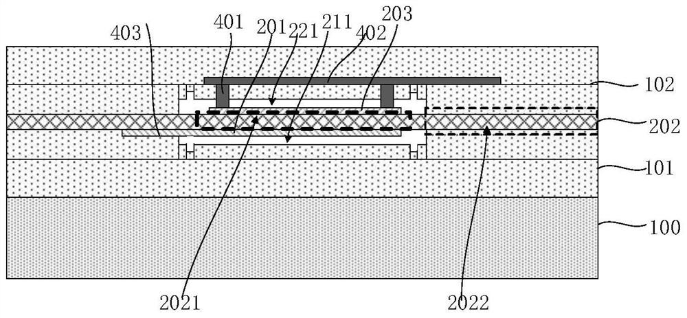
[0041] Embodiment 1 of the present invention provides a thin film bulk acoustic resonator, figure 1 It is a structural schematic diagram of the thin film bulk acoustic resonator in Embodiment 1 of the present invention, please refer to figure 1 , the thin film bulk acoustic resonator includes:
[0042] The stacked extraction electrode 201, the piezoelectric layer 202 and the external electrode 203, the effective resonance area includes the area where the extraction electrode 201, the piezoelectric layer 202 and the external electrode 203 overlap each other in a direction perpendicular to the surface of the piezoelectric layer 202, The outside of the effective resonance area is an invalid area;
[0043] A first dielectric layer 101, a first gap 211 is provided between the surface of the first dielectric layer 101 and the surface of the extraction electrode 201;
[0044] A second dielectric layer 102, a second gap 221 is provided between the surface of the second dielectric la...
Embodiment 2
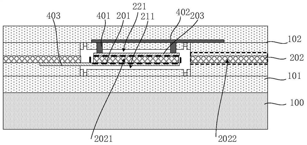
[0060] Embodiment 2 of the present invention provides a thin film bulk acoustic resonator, figure 2 It is a schematic structural diagram of a thin film bulk acoustic resonator in Embodiment 2 of the present invention. The difference between this embodiment and Embodiment 1 is that in this embodiment, the resonant part 2021 of the piezoelectric layer 202 is located in the effective resonant region, and the overlapping part 2022 is located in the Outside the effective resonance area, the resonance part 2021 and the overlapping part 2022 are separated from each other. Please refer to figure 2 , the specific structure is as follows:
[0061] The first gap 211 and the second gap 221 communicate with each other to form a cavity, the resonant part 2021 is completely located in the cavity, the overlapping part 2022 is located outside the cavity, and the overlapping part 2022 and the resonant part 2021 are completely separated, so that the outer circumference of the resonant part 20...
Embodiment 3
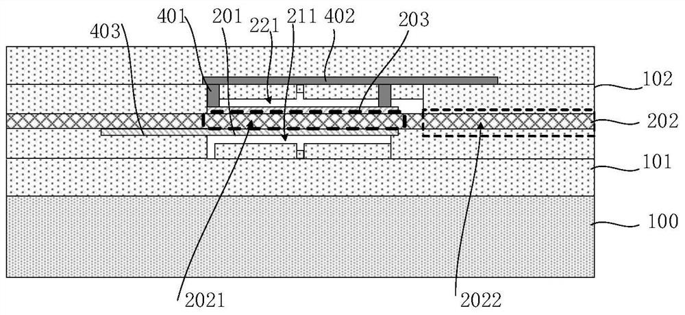
[0063] Embodiment 3 of the present invention provides a thin film bulk acoustic resonator, image 3 It is a schematic structural diagram of a thin-film bulk acoustic resonator according to Embodiment 3 of the present invention. The difference between this embodiment and Embodiment 1 is that the piezoelectric layer 202 is a complete film layer, and the overlapping part 2022 and the resonance part 2021 are connected together. One structure. A part of the conductive column 401 is located at the edge of the second gap 221 and is in contact with the second dielectric layer 102 , and a part is located in the second gap 221 with a distance from the boundary of the second gap 221 . The conductive pillars 401 can also all be located at the edge of the second gap 221, or the conductive pillars 401 are not in contact with the edge of the second gap 221.
[0064] In the above embodiments 1 to 3, the external electrodes are located above the lead-out electrodes, but in these embodiments, ...
PUM
 Abstract
Description
Claims
Application Information


