
EMI shielding film and method of manufacturing the same

A technology of anti-electromagnetic interference and production method, which is applied in the direction of film/sheet adhesives, electrical components, conductive adhesives, etc., can solve the problems of electromagnetic wave shielding ability and thermal conductivity cannot be improved, and achieve flatness, Both flexibility and bending resistance, heat resistance, and adhesive strength are combined

Pending Publication Date: 2022-01-25
NANOBIT TECH
View PDF0 Cites 0 Cited by
  • Summary
  • Abstract
  • Description
  • Claims
  • Application Information

AI Technical Summary

Problems solved by technology

[0004] The technical problem to be solved by the present invention is to provide an anti-electromagnetic interference film, which can solve the problem that the electromagnetic wave shielding ability and heat conduction ability of the prior art cannot be improved, and achieve the purpose of taking into account the adhesion strength, heat resistance and electrical reliability at the same time

Method used


Image

  • EMI shielding film and method of manufacturing the same
  • EMI shielding film and method of manufacturing the same
  • EMI shielding film and method of manufacturing the same

Examples


Embodiment 1

[0060] Prepare the acrylate solution first, mix 12.5 grams of polyalkylacrylate compound and 22.5 grams of ethyl acetate (EAC) at room temperature, use a 300 ml three-port glass reactor, and stir evenly with a stirrer with 2 impellers. After stirring for two hours, add 35.0 grams of dibasic acid ester solution, 25 g of solvent (toluene), 3 grams of nickel particle powder (more than 50% of the particle size is 5-10 μm), and 2 parts by weight of dispersant , PEDOT:PSS with a concentration of 1 to 2.5% and 0.5 grams, kept stirring at room temperature for eight hours and then allowed to stand for one hour, and then added EAC or toluene as needed to adjust the viscosity to control the viscosity of the conductive adhesive composition at 30cps~ 50cps. The ingredients are shown in Table 1. After production, the resin composition is coated on the flexible composite metal layer at room temperature by Die Coater mold coating method. After coating, the surface is dried by heating. The he...

Embodiment 2

[0062] Resin composition 2 was prepared in the same manner as in Example 1, except that the amount of polyalkylacrylate compound in the acrylate solution was adjusted to 10 g and the weight of EAC to 25 g, as shown in Table 1.

Embodiment 3

[0064]Resin composition 3 was prepared in the same manner as in Example 1, except that the amount of polyalkylacrylate compound in the acrylate solution was adjusted to 14 grams and the weight of EAC to 21 grams, as shown in Table 1.


PUM

PropertyMeasurementUnit
particle diameteraaaaaaaaaa
thicknessaaaaaaaaaa
thicknessaaaaaaaaaa

Abstract

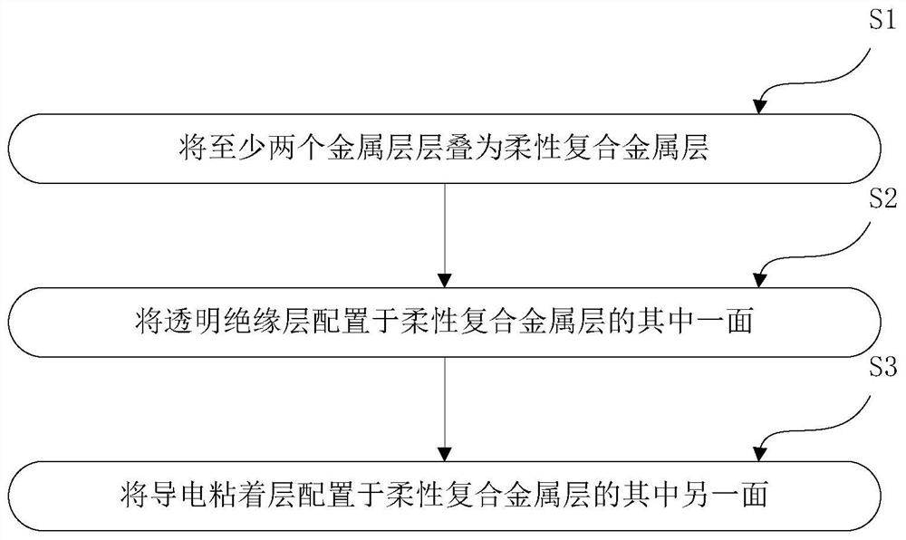
An EMI shielding film includes a flexible composite metal layer, a transparent insulating layer, and a conductive adhesive layer. The conductive adhesive layer is formed by removing a solvent from a conductive adhesive composition. The conductive adhesive composition includes an acrylate solution, a divalent acid ester solution, a plurality of conductive particles, and the solvent. The present disclosure further includes a method of manufacturing the EMI shielding film.

Description

technical field [0001] The invention relates to an anti-electromagnetic interference film and a manufacturing method thereof, in particular to an anti-electromagnetic interference film and a manufacturing method thereof that can take both adhesive strength and electrical reliability into consideration. Background technique [0002] With the development of electronic products and the miniaturization trend of electronic products, flexible printed circuit boards are becoming more and more important. Especially for office machines, communication machines, and mobile electronic products, the electromagnetic interference problem that needs to be dealt with for multi-function, high performance, and miniaturization is more important. Therefore, an electromagnetic wave shielding film for shielding electromagnetic noise is generally designed on many flexible printed circuit boards. However, the electromagnetic wave shielding film in the prior art must be able to be attached to irregu...

Claims


Application Information

Patent Timeline
Patent Type & Authority Applications(China)
IPC IPC(8): H05K9/00
CPCH05K9/0086H05K9/0083H05K9/0088C09J7/29C09J9/02C09J2301/314C09J2400/163C09J2433/00C09J2301/408C08K2201/001
Inventor 黄松建张裕洋刘修铭游秉丰
Owner NANOBIT TECH
Learn More