
Back grinding tape

A back-grinding, one-side technology, used in abrasives, bulk chemical production, manufacturing tools, etc., can solve the problems of semiconductor wafer circuit damage and foreign matter attached to semiconductor wafers

Pending Publication Date: 2022-01-28
株式会社力森诺科
View PDF9 Cites 0 Cited by
  • Summary
  • Abstract
  • Description
  • Claims
  • Application Information

AI Technical Summary

Problems solved by technology

[0005] In addition, conventionally, when peeling the back grinding tape from the semiconductor wafer, static electricity called peeling electrification may be generated, and the circuit of the semiconductor wafer may be destroyed, or foreign matter may adhere to the semiconductor wafer.

Method used


Image

  • Back grinding tape

Examples


Embodiment

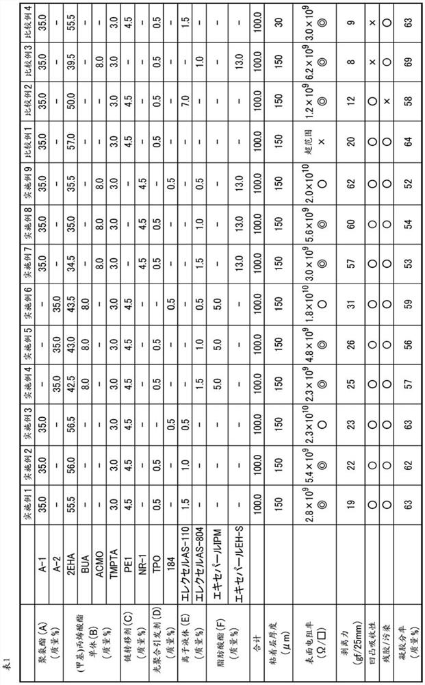
[0206] Hereinafter, the present invention will be described more concretely by way of examples and comparative examples. In addition, the present invention is not limited only to the following examples.

[0207]

[0208] In a reactor equipped with a thermometer, a stirrer, a dropping funnel, and a cooling pipe with a drying pipe, 0.55 kg of a hydrogenated product of diphenylmethane diisocyanate (Desmogluer W, manufactured by Sumika Cobestorouletan) was added ( 2.1 mol), 4.01 kg (2.0 mol) of polypropylene glycol (Actocol D-2000; produced by Mitsui Chemicals, number average molecular weight 2000) having a hydroxyl group at the end with a hydroxyl value of 56 mgKOH / g, and di Octyltin (Neostan U-810, manufactured by Nitto Kasei Co., Ltd.) 0.8 g.

[0209] Then, the temperature of the reactor was raised to 60° C. and the reaction was carried out for 4 hours to obtain a polyurethane having isocyanate groups at both terminals as a precursor of the polyurethane (A). Next, 23.22 g (...


PUM

PropertyMeasurementUnit
thicknessaaaaaaaaaa
melting pointaaaaaaaaaa
thicknessaaaaaaaaaa

Abstract

A back grinding tape having a sheet-shaped substrate and an adhesive agent layer formed on one surface of the substrate, wherein the adhesive agent layer comprises a cured product of an adhesive agent composition and is 50-500 [mu]m thick, the adhesive agent composition includes a polyurethane (A), a (meth)acrylate monomer (B), a chain transfer agent (C), a photopolymerization initiator (D), and 0.4-6 mass% of an ionic liquid (E), and the polyurethane (A) includes a polyurethane (a1) having a skeleton that includes a structure derived from a polyoxyalkylene polyol and a structure derived from a polyisocyanate, and having (meth)acryloyl groups at a plurality of ends.

Description

technical field [0001] The present invention relates to a back grinding tape suitable for use in semiconductor wafer processing. [0002] This application claims priority based on Japanese Patent Application No. 2019-162092 filed in Japan on September 5, 2019, and the content thereof is incorporated herein. Background technique [0003] In accordance with the demand for thinning semiconductor devices, a back grinding process of semiconductor wafers is performed in the manufacturing process of semiconductor devices. In the back grinding process of the semiconductor wafer, after the surface (front surface) of the semiconductor wafer is protected with a back grinding tape, the back surface of the semiconductor wafer is ground to reduce the thickness of the semiconductor wafer. [0004] Conventionally, various back grinding tapes used to protect the surface of a semiconductor wafer have been proposed. In recent years, backgrinding tapes having sufficient unevenness absorption ...

Claims


Application Information

Patent Timeline
Patent Type & Authority Applications(China)
IPC IPC(8): B24D11/00B24D11/02
CPCB24D11/00B24D11/02H01L21/304C09J11/06C09J7/38C09J175/04Y02P20/54C09J175/14
Inventor 池谷达宏中西健一
Owner 株式会社力森诺科
Learn More