
Tape for semiconductor processing

A semiconductor and main body technology, applied in semiconductor/solid-state device manufacturing, adhesive additives, non-polymer adhesive additives, etc., can solve the problem of poor adhesion of parts, changes in physical properties of adhesives, and adjustments or changes in physical properties of adhesives over time. Suppressing difficulties and other problems to achieve the effect of sufficient antistatic performance

Pending Publication Date: 2022-07-08
株式会社力森诺科
View PDF7 Cites 0 Cited by
  • Summary
  • Abstract
  • Description
  • Claims
  • Application Information

AI Technical Summary

Problems solved by technology

However, if a material having an antistatic effect such as a surfactant, a conductive filler, and carbon black is added to the adhesive itself, the physical properties of the adhesive change.
In addition, it becomes difficult to adjust or suppress stickiness properties and changes over time
Further, when the adhesive tape is peeled off, the adhesive and the added antistatic material may move to the adherend and contaminate the adherend
In this case, on the surface of the adherend, the adhesion of residual glue visible to the naked eye, particulate matter at the microscopic level, or liquid that cannot be observed optically occurs, which may cause adhesion of parts in subsequent processes. Possibility of adverse effects such as adverse

Method used


Image

  • Tape for semiconductor processing
  • Tape for semiconductor processing

Examples


manufacture example 1

[0209]

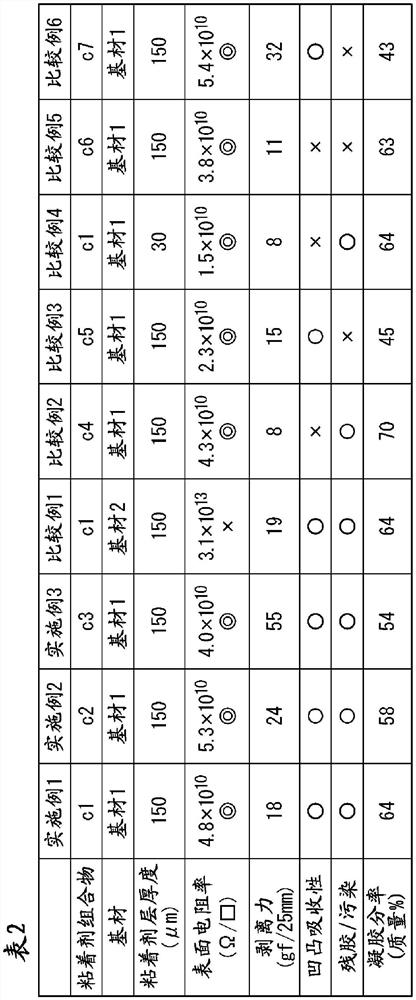
[0210] 9.4 parts by mass of polypyrrole dispersion (PPY-12 manufactured by Maruhi Oil & Chemical Industry Co., Ltd., solid content 8%), polyester-based binder (BI-12 manufactured by Maruhi Oil & Chemical Industry Co., Ltd., solid content 30%) ) 5.0 parts by mass, 2.6 parts by mass of a melamine-based crosslinking agent (CL-12 manufactured by Maruhi Oil Chemical Industry Co., Ltd., solid content 25%), 0.05 parts by mass of polyoxyethylene lauryl ether, and 830.0 parts by mass of water to prepare water Dispersions. Next, as a substrate main body, a 50 μm-thick PET film (manufactured by Toyobo Co., Ltd., trade name: Esther (trademark) film E5100) was coated with a gravure coater so that the film thickness after heat curing became 1.0 μm. The resin composition is applied. Next, the sheet-like base material 1 was obtained by performing hardening at 130 degreeC for 1 minute. The resistance of the base material 1 measured by a low resistivity meter (Rolesta-AX manufactur...

Synthetic example 1

[0215]

[0216] In a reactor equipped with a thermometer, a stirrer, a dropping funnel, and a cooling tube with a drying tube, 0.55 kg (2.1 kg) of a hydrogenated product of diphenylmethane diisocyanate (Destroy W, manufactured by Sumika Co., Ltd.) mol), 4.01 kg (2.0 mol) of polypropylene glycol having a hydroxyl group at the terminal with a hydroxyl value of 56 mgKOH / g (Actoko D-2000; manufactured by Mitsui Chemicals, number average molecular weight 2000), and dioctyltin as a urethane catalyst (ネオスタン U-810, manufactured by Nitto Chemical Co., Ltd.) 0.8 g.

[0217] Then, the temperature of the reactor was raised to 60° C. and the reaction was carried out for 4 hours to obtain a polyurethane having isocyanate groups at both ends as a precursor of the polyurethane (A). Next, 23.22 g (0.2 mol) of 2-hydroxyethyl acrylate was added to the reactor, and the temperature was raised to 70° C. and reacted for 2 hours to obtain 4.58 kg of polyurethane (A-1) having a mass average molecula...

Synthetic example 2

[0220]

[0221] The method for synthesizing polyurethane (A-1) was the same as the method for synthesizing polyurethane (A-1), except that 2.1 mol of isophorone diisocyanate (Destroyd I, manufactured by Sumina Chemical Co., Ltd.) was used instead of the hydrogenated product of diphenylmethane diisocyanate. By operation, polyurethane (A-2) having a mass average molecular weight of 66,000 was obtained.

[0222] The obtained polyurethane (A-2) was analyzed by infrared absorption spectroscopy (IR). As a result, the peak derived from the isocyanate group was not observed. Therefore, it was confirmed that the urethane (A-2) was the urethane (a1) in which acryloyloxy groups were introduced into all the terminals.

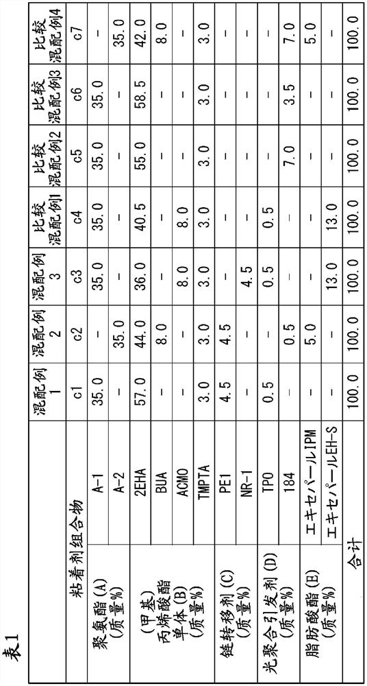
[0223] (Compounding Examples 1 to 3, Comparative Compounding Examples 1 to 4)

[0224]

[0225] The polyurethane (A) obtained by the above-mentioned synthesis method, the (meth)acrylate monomer (B) shown in Table 1, the chain transfer agent (C), the photopolymerizati...


PUM

PropertyMeasurementUnit
thicknessaaaaaaaaaa
thicknessaaaaaaaaaa
thicknessaaaaaaaaaa

Abstract

Provided is a tape for semiconductor processing, which has sufficient concave-convex absorbency, moderate adhesive force and antistatic performance, is less susceptible to the occurrence of adhesive residues after the tape for semiconductor processing is peeled off, and can be manufactured by a small number of manufacturing steps. The tape for semiconductor processing has a sheet-like base material and an adhesive layer, wherein the sheet-like base material has an antistatic layer provided on at least one surface of a base material main body. The antistatic layer contains a polypyrrole compound. The adhesive layer is a cured product of an adhesive composition and has a thickness of 50-500 [mu] m. The adhesive composition contains a polyurethane (A), a (meth) acrylate monomer (B) containing a compound having a (meth) acryloyloxy group, a chain transfer agent (C), and a photopolymerization initiator (D). The polyurethane (A) contains a polyurethane (a1) having (meth) acryloyl groups at a plurality of terminals.

Description

technical field [0001] The present invention relates to a belt for semiconductor processing. Background technique [0002] With the demand for thinning of semiconductor devices, a back grinding process of semiconductor wafers is performed in the manufacturing process of semiconductor devices. In the back grinding step of the semiconductor wafer, after the surface of the semiconductor wafer is protected with a back grinding tape, the back surface is ground to reduce the thickness of the semiconductor wafer. [0003] This application claims priority based on Japanese Patent Application No. 2019-227280 filed in Japan on December 17, 2019, the content of which is incorporated herein by reference. [0004] Various back grinding tapes used to protect the surface of a semiconductor wafer have been proposed in the past. In recent years, a back grinding tape has been required to have sufficient unevenness absorption even for semiconductor wafers having uneven surfaces such as semic...

Claims


Application Information

Patent Timeline
Patent Type & Authority Applications(China)
IPC IPC(8): C09J7/20
CPCB32B27/00C08F290/06C09J4/00C09J7/38C09J7/20C09J11/06C09J175/08C09J175/16H01L21/304C09J2203/326
Inventor 池谷达宏中西健一
Owner 株式会社力森诺科
Learn More