Cleaning brush assembly and wafer cleaning device

A technology for cleaning brushes and components, applied in cleaning methods and utensils, electrical components, chemical instruments and methods, etc., can solve problems such as wafer secondary pollution, pollutant leakage, and affecting cleaning effects

Pending Publication Date: 2022-02-01
HWATSING TECH
View PDF1 Cites 1 Cited by
  • Summary
  • Abstract
  • Description
  • Claims
  • Application Information

AI Technical Summary

Problems solved by technology

[0005] However, the existing roller brush structure is unreasonable, and there is a problem of...

Method used


Image

  • Cleaning brush assembly and wafer cleaning device
  • Cleaning brush assembly and wafer cleaning device
  • Cleaning brush assembly and wafer cleaning device

Examples


Embodiment Construction

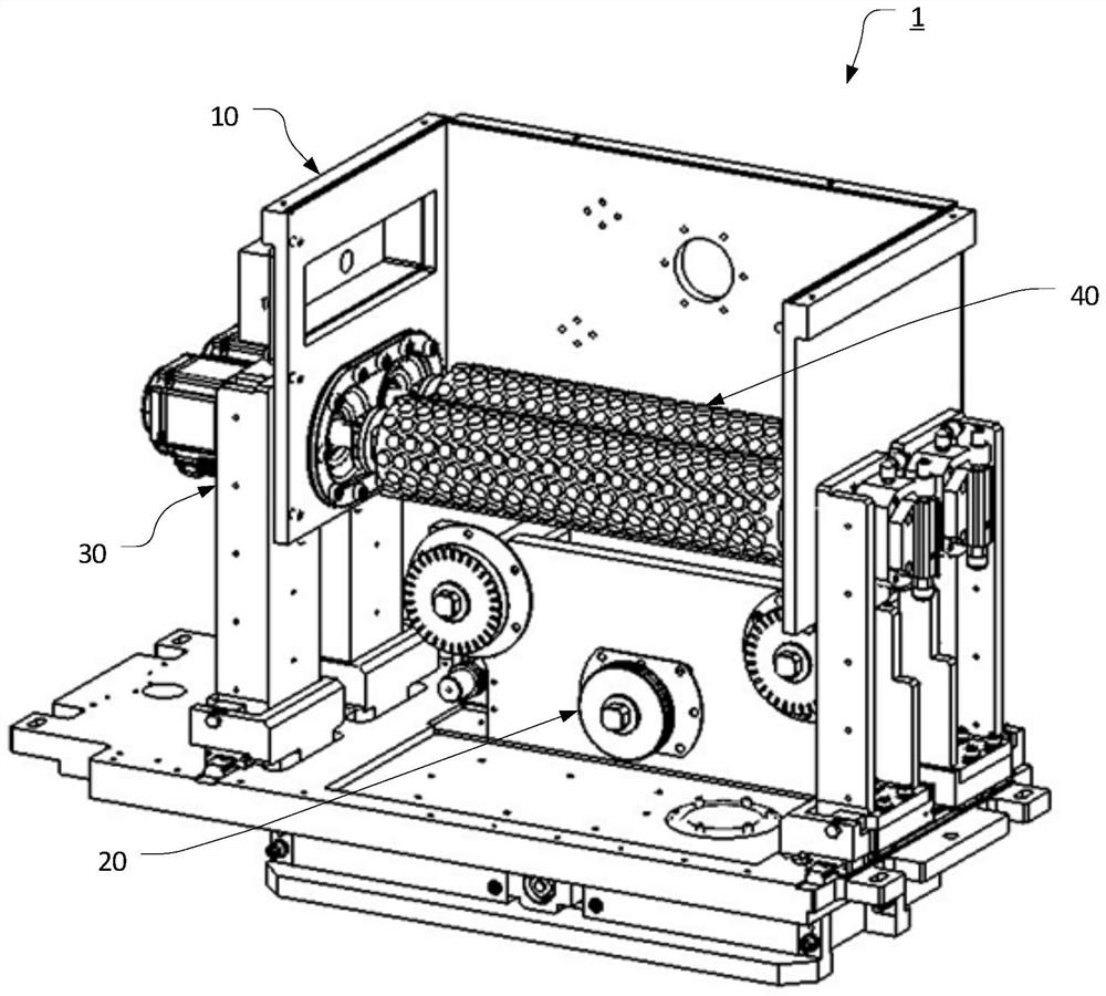
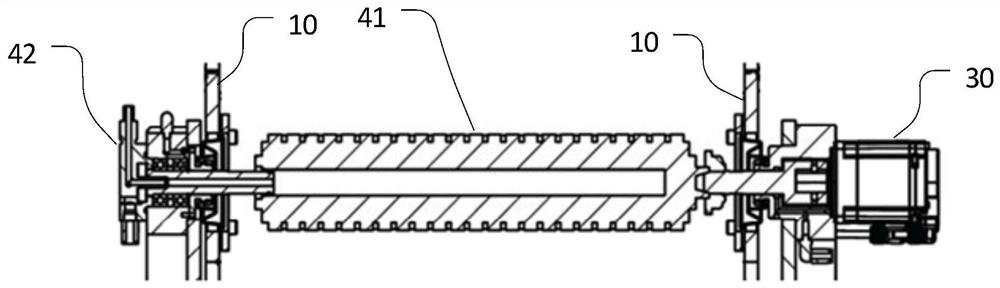
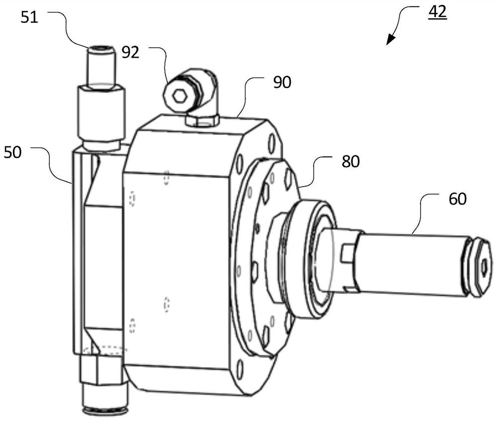
[0028] The technical solutions of the present invention will be described in detail below in conjunction with specific embodiments and accompanying drawings. The examples described here are specific implementations of the present invention and are used to illustrate the concept of the present invention; these descriptions are all explanatory and exemplary, and should not be construed as limiting the implementation of the present invention and the protection scope of the present invention . It should be noted that, in the case of no conflict, the embodiments in the present application and the features in the embodiments can be combined with each other. In addition to the embodiments described here, those skilled in the art can also adopt other obvious technical solutions based on the claims of the application and the contents disclosed in the specification, and these technical solutions include adopting any modifications made to the embodiments described here. Obvious alternat...


PUM

PropertyMeasurementUnit
Widthaaaaaaaaaa

Abstract

The invention discloses a cleaning brush assembly and a wafer cleaning device, the cleaning brush assembly comprises a cleaning brush and a liquid inlet mechanism connected to one end of the cleaning brush, and the liquid inlet mechanism comprises a liquid inlet end cover, a follow-up shaft and a bearing assembly; the liquid inlet end cover is provided with a liquid inlet end, one side of the liquid inlet end cover is provided with an extending thin shaft and an annular side wall surrounding the thin shaft, an annular groove is formed between the thin shaft and the annular side wall, and the thin shaft is hollow and is communicated with the liquid inlet end through a first passage in the liquid inlet end cover; one end of the follow-up shaft is arranged on the peripheral side of the thin shaft in a sleeving mode and stretches into the annular groove so that the thin shaft can be inserted into a center through hole of the follow-up shaft, the other end of the follow-up shaft stretches into the cleaning brush, and the center through hole penetrates through the follow-up shaft so that the first channel can be communicated with the cleaning brush, and therefore liquid can be led into the cleaning brush; and the bearing assembly is arranged on the peripheral side of the follow-up shaft in a sleeving mode.

Description

technical field [0001] The invention relates to the technical field of semiconductor wafer processing, in particular to a cleaning brush assembly and a wafer cleaning device. Background technique [0002] In the semiconductor field, the cleanliness of the wafer surface is one of the important factors affecting the reliability of semiconductor devices. During the wafer manufacturing process, such as: deposition, plasma etching, photolithography, electroplating, etc., it is possible to introduce contamination and / or particles on the wafer surface, resulting in a decrease in the cleanliness of the wafer surface, and the manufactured semiconductor devices are good. The rate is not high. Chemical Mechanical Planarization (CMP) is a global planarization ultra-precision surface processing technology. Due to the large amount of chemical reagents and abrasives used in chemical mechanical polishing, a large amount of pollutants such as abrasive particles and grinding by-products wil...

Claims


Application Information

Patent Timeline
IPC IPC(8): H01L21/67B08B1/02B08B3/02B08B3/08
CPCH01L21/67046B08B1/002B08B1/02B08B3/022B08B3/08
Inventor 申兵兵王江涛李长坤
Owner HWATSING TECH
Why Eureka
Try Eureka