DDR micro-module structure based on TSV wafer reconstruction and multi-layer stacking and preparation technology

A multi-layer stacking and preparation technology, applied in semiconductor/solid-state device manufacturing, electrical components, electrical solid-state devices, etc., to achieve the effect of solving heat concentration, solving complex wiring, and facilitating connection and use

Pending Publication Date: 2022-02-01
XIAN MICROELECTRONICS TECH INST
View PDF2 Cites 0 Cited by
  • Summary
  • Abstract
  • Description
  • Claims
  • Application Information

AI Technical Summary

Problems solved by technology

This method has the following problems: Due to the limitation of the stack height, the thickness of the gasket 4 used for the stack is generally about 500 μm, and silicon wafers are generally used as the stack gasket
This solution is similar to the above-mentioned solution, but the RDL process is omitted, and it still cannot solve the problem of exponential growth of the fan-out area of ​​the bonding wire 5 and the problem of heat concentration as the number of stacked layers increases.

Method used


Image

  • DDR micro-module structure based on TSV wafer reconstruction and multi-layer stacking and preparation technology
  • DDR micro-module structure based on TSV wafer reconstruction and multi-layer stacking and preparation technology
  • DDR micro-module structure based on TSV wafer reconstruction and multi-layer stacking and preparation technology

Examples


Embodiment Construction

[0034] In order to make the purpose, technical solutions and advantages of the embodiments of the present invention clearer, the technical solutions of the present invention will be clearly and completely described below in conjunction with the accompanying drawings. Obviously, the described embodiments are part of the embodiments of the present invention, not all of them. the embodiment. Based on the embodiments of the present invention, all other embodiments obtained by persons of ordinary skill in the art without making creative efforts belong to the protection scope of the present invention.

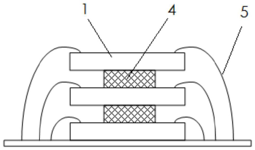
[0035] As a specific embodiment of the present invention, such as Figure 5 As shown, a DDR micromodule structure based on TSV wafer reconstruction and multi-layer stacking includes a multi-layer TSV silicon substrate 6. In this embodiment, there are five layers of TSV silicon substrates 6, and two adjacent layers of TSV silicon substrates 6 A plurality of micro-bumps 7 are used for...


PUM

PropertyMeasurementUnit
Thicknessaaaaaaaaaa

Abstract

The invention discloses a DDR micro-module structure based on TSV wafer reconstruction and multi-layer stacking and a preparation technology. The DDR micro-module structure comprises multiple layers of TSV silicon substrates, and every two adjacent layers of TSV silicon substrates are connected through a plurality of micro convex points; a cavity is formed in the upper end face of each layer of TSV silicon substrate, a DDR bare chip is embedded in each cavity, and a PAD of each DDR bare chip faces upwards; and the via hole or BUMP of each layer of TSV silicon substrate is connected with the PAD of the DDR bare chip embedded in the TSV silicon substrate through RDL wiring. The problem that the fan-out area of the bonding wire is increased in an exponential level mode due to increase of the number of stacked layers is effectively solved.

Description

technical field [0001] The invention belongs to the field of multi-component integration of microsystems, and in particular relates to a DDR micromodule structure and preparation process based on TSV wafer reconstruction and multi-layer stacking. Background technique [0002] DDR (Double Data Rate Synchronous Dynamic Random Access Memory) is SDRAM with double data transfer rate, its data transfer speed is twice the system clock frequency, due to the increased speed, its transfer performance is better than traditional SDRAM, widely used In high-performance servers, desktops, notebooks, and other devices. However, subject to the constraints of the tape-out process, such as figure 1 As shown, the external bonding PAD 2 on the DDR bare chip 1 is in the middle position, and this structure is not conducive to the stacking of the DDR bare chip. like figure 2 As shown, the industry generally adopts the RDL (Redistribution Layer, rewiring) method to redistribute the PAD 2 to the ...

Claims


Application Information

Patent Timeline
IPC IPC(8): H01L25/065H01L23/48H01L21/50H01L21/56H01L21/60
CPCH01L25/0657H01L23/481H01L21/50H01L21/56H01L24/81H01L2224/81H01L2224/81801
Inventor 匡乃亮唐磊赵超郭雁蓉刘宗溪杨巧
Owner XIAN MICROELECTRONICS TECH INST
Why Eureka
Try Eureka