Check patentability & draft patents in minutes with Patsnap Eureka AI!

Manufacturing method of shield gate trench type semiconductor device

A manufacturing method and semiconductor technology, applied in semiconductor/solid-state device manufacturing, semiconductor devices, electrical components, etc., can solve problems such as high costs and achieve the effect of reducing process costs

Pending Publication Date: 2022-02-08
SHANGHAI HUAHONG GRACE SEMICON MFG CORP
View PDF0 Cites 1 Cited by
  • Summary
  • Abstract
  • Description
  • Claims
  • Application Information

AI Technical Summary

Problems solved by technology

[0027] It can be seen from the above that the existing method needs to use a single photolithography process to lead the source out of the top protection of the trench in step three, which has a relatively high cost

Method used


Image

  • Manufacturing method of shield gate trench type semiconductor device
  • Manufacturing method of shield gate trench type semiconductor device
  • Manufacturing method of shield gate trench type semiconductor device

Examples


Embodiment Construction

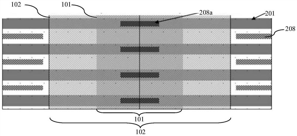
[0072] Such as image 3 As shown, it is a flow chart of the manufacturing method of the shielded gate trench 401 type semiconductor device according to the embodiment of the present invention; Figure 4 As shown, it is the layout structure adopted by the manufacturing method of the shielded gate trench 401 type semiconductor device according to the embodiment of the present invention; Figure 4A shown, is Figure 4 Enlarged view of the lead-out structure of Zhongyuan polysilicon; Figure 5A to Figure 5F As shown, it is a schematic diagram of the device structure in each step of the manufacturing method of the shielded gate trench 401 type semiconductor device according to the embodiment of the present invention; the manufacturing method of the shielded gate trench 401 type semiconductor device according to the embodiment of the present invention includes the following steps:

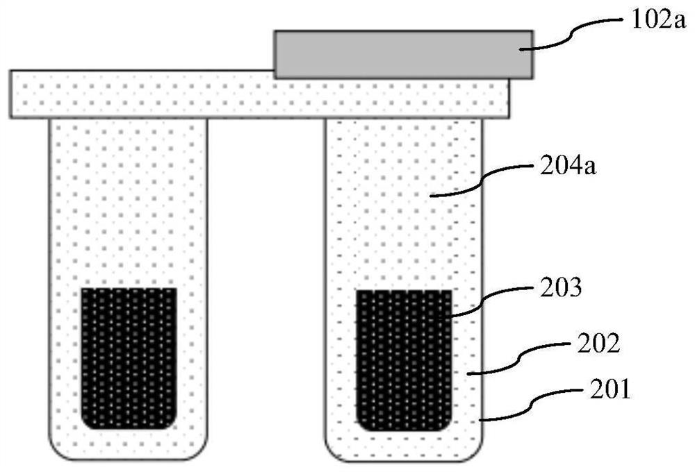
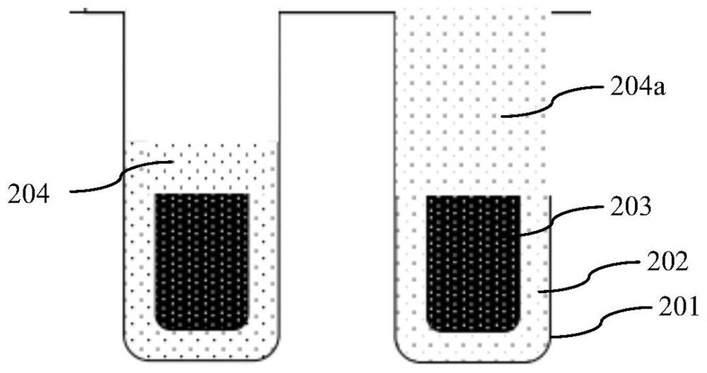
[0073] Step 1, such as Figure 5A As shown, a plurality of trenches are formed on a semiconductor ...


PUM


Abstract

The invention discloses a manufacturing method of a shield gate trench type semiconductor device, and the method comprises the following steps: 1, forming a plurality of trenches, and defining the width of a source lead-out trench to meet the following relational expression: CDL > CDCT + 2 * Tpoly + OVLCT, wherein the width of the gate trench meets the following relational expression: CDC is less than 2 * Tpoly; 2, forming a bottom dielectric layer and source polysilicon; 3, forming an inter-polycrystalline silicon oxide layer in each trench at the same time; 4, forming a gate dielectric layer; 5, performing polycrystalline silicon deposition to form a second polycrystalline silicon layer; 6, performing back etching on the second polycrystalline silicon layer, forming a polycrystalline silicon gate by the second polycrystalline silicon layer which is filled in the gate groove after back etching, and reserving the residual second polycrystalline silicon layer on the side surface of the source lead-out groove. 7, growing a dielectric layer under metal; 8, performing etching to form an opening of the contact hole and filling metal. According to the invention, the number of masks for forming IPO can be reduced, so that the process cost can be reduced.

Description

technical field [0001] The invention relates to a method for manufacturing a semiconductor integrated circuit, in particular to a method for manufacturing a shielded gate trench type (SGT) semiconductor device. Background technique [0002] The source polysilicon (Source Poly) is introduced into the SGT to assume the role of the charge-coupled (Charge-Coupled) structure in the MOSFET. Therefore, in the device design, it is necessary to increase the source polysilicon extraction (Source Poly Linkup) area to extract the polysilicon located in the gate trench. The source polysilicon (Source Poly) under the gate (Gate Poly). [0003] In the SGT manufacturing process flow, the formation of the Source Poly linkup structure usually requires 3 to 4 layers of lithography, respectively Trench / (Poly1) / P-cover / Contact, where Trench means trench lithography, and Poly1 means polysilicon The lithography of the gate, P-cover means the lithography of the interpolysilicon oxide layer (IPO), ...

Claims


Application Information

Patent Timeline
IPC IPC(8): H01L21/336H01L21/28
CPCH01L29/66484H01L29/66666H01L21/28035H01L21/28123
Inventor 顾昊元蔡晨李亮
Owner SHANGHAI HUAHONG GRACE SEMICON MFG CORP
Features
  • R&D
  • Intellectual Property
  • Life Sciences
  • Materials
  • Tech Scout
  • Unparalleled Data Quality
  • Higher Quality Content
  • 60% Fewer Hallucinations
Learn More