
High off-impedance drive circuit for suppressing sic MOSFET crosstalk

A driving circuit and clamping circuit technology, applied in the direction of high-efficiency power electronic conversion, electronic switches, electrical components, etc., can solve the problems of inability to solve the common source parasitic inductance effect, increase the difficulty of system layout, etc., to maintain safe and reliable operation, The effect of solving the crosstalk voltage problem

Active Publication Date: 2022-03-29
NANTONG UNIVERSITY
View PDF0 Cites 0 Cited by
  • Summary
  • Abstract
  • Description
  • Claims
  • Application Information

AI Technical Summary

Problems solved by technology

For parasitic inductance L s For the introduced crosstalk voltage, the method of shortening the length of SiC MOSFET package pins is generally adopted, which will increase the difficulty of system layout
It is also possible to use decoupling capacitors to eliminate part of the common source parasitic inductance, but this method cannot solve the influence of the common source parasitic inductance in the package

Method used


Image

  • High off-impedance drive circuit for suppressing sic MOSFET crosstalk
  • High off-impedance drive circuit for suppressing sic MOSFET crosstalk
  • High off-impedance drive circuit for suppressing sic MOSFET crosstalk

Examples


Embodiment Construction

[0028] The present invention will be further explained below in conjunction with the accompanying drawings.

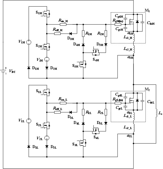
[0029] Such as figure 1 As shown, a high off-impedance driving circuit for suppressing crosstalk of SiC MOSFETs includes a complementary conduction SiC MOSFET upper bridge arm and a SiC MOSFET lower bridge arm, and each bridge arm includes a basic driving circuit and a clamping circuit respectively.

[0030] The basic drive circuit for the upper arm of a SiC MOSFET consists of a supply voltage source V 1H , supply voltage source V 2H ,turning tube S 1H ,turning tube S 2H , turn-on gate resistance R on_H , turn-off gate resistance R off_H ,diode D 1H ,diode D 2H ,diode D 3H . supply voltage source V 1H positive pole and switching tube S 1H connected to the drain of the supply voltage source V 1H cathode and diode D 1H connected to the negative pole; the switch tube S 1H The source and gate resistance of the turn-on R on_H One end and the sw...


PUM


Abstract

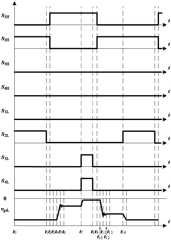
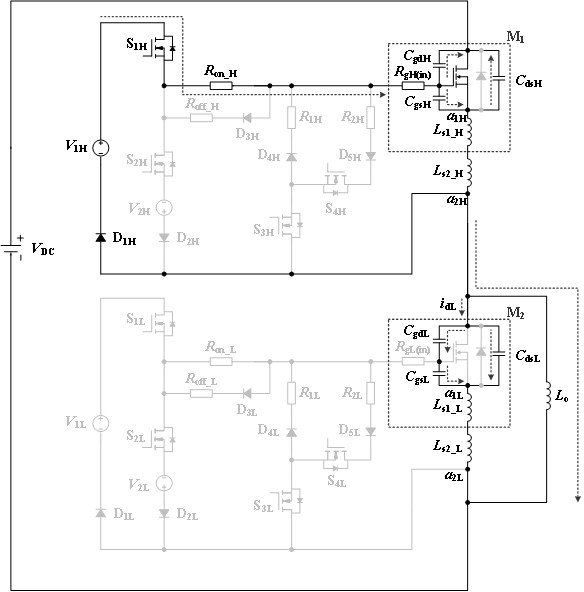
The invention discloses a high turn-off impedance driving circuit for suppressing crosstalk of SiC MOSFETs, which comprises an upper bridge arm of SiC MOSFET and a lower bridge arm of SiC MOSFET with complementary conduction, and each bridge arm respectively includes a basic driving circuit and a clamping circuit; The basic driving circuit precharges the negative voltage for the gate-source capacitance of the passive tube to prevent false conduction during positive crosstalk, and the clamping circuit is used to discharge the charge of the gate-source capacitor of the passive tube to prevent negative crosstalk during negative crosstalk. to the breakdown. The beneficial effects of the present invention are: offsetting the gate-drain capacitance by adjusting the gate-source voltage C gd the transfer charge. During the switching process of the active tube, the gate and source of the passive tube do not form a loop, that is, the high off-impedance state, and the common source parasitic inductance L s The introduced crosstalk voltage will not be loaded across the gate-source. Solve the gate-to-drain capacitance at the same time C gd and common source parasitic inductance L s Introduced crosstalk voltage.

Description

technical field [0001] The invention relates to a driving circuit for suppressing SiC MOSFET crosstalk. Background technique [0002] SiC MOSFET has the advantages of high switching frequency, low switching loss, and high temperature resistance. In the current field of power electronics, SiC MOSFETs are often used in high frequency, high power density, high temperature and other occasions. However, as the switching speed increases, the crosstalk phenomenon becomes more and more serious. This is because during the turn-on and turn-off process of the active tube, the drain-source voltage of the passive tube changes rapidly (that is, d v / d t rapid change), d v / d t Acting on the gate-drain parasitic capacitance of the passive transistor C gd causes a current displacement, when part of the displacement current flows through the gate-source parasitic capacitance C gs , the crosstalk problem occurs. The commonly used TO-247-3 package SiC MOSFET also has a large common-s...

Claims


Application Information

Patent Timeline
Patent Type & Authority Patents(China)
IPC IPC(8): H03K17/16H03K17/687H02M1/088H02M1/44H02M1/32
CPCH03K17/165H03K17/6872H02M1/088H02M1/44H02M1/32H03K2217/0081Y02B70/10
Inventor 张雷吴典桑顺任磊秦岭黄杰杰茅靖峰郭晓丽柏树根
Owner NANTONG UNIVERSITY
Learn More