Circuit board for energy-saving fan and energy-saving fan
A circuit board, energy-saving technology, applied in the direction of printed circuits, circuit devices, printed circuit components, etc., can solve the problems of large loss and inability to shield external signals
- Summary
- Abstract
- Description
- Claims
- Application Information
AI Technical Summary
Problems solved by technology
Method used
Image
Examples
Embodiment 1
[0056] An embodiment of the present invention provides a circuit board for an energy-saving fan, please refer to figure 1 , the present invention provides a technical solution, comprising: a packaging case 1, a circuit board body, the circuit board body is arranged inside the packaging case 1, the circuit board body includes: a shielding layer, and a connection structure is connected to the packaging case 1 101. The connection structure 101 is electrically connected to the circuit board body.
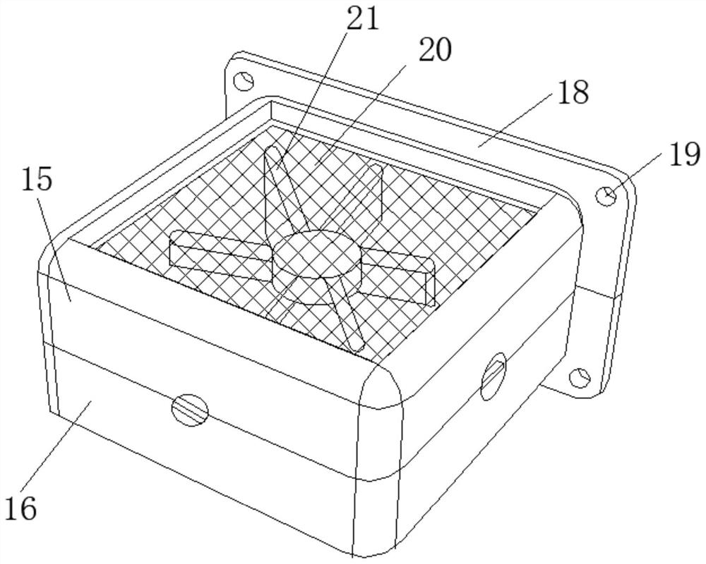
[0057] Preferably, heat conducting fins 17 are arranged on the side of the circuit board body for heat dissipation. power consumption, and accelerate the aging and deformation of the circuit board itself, the present invention arranges a heat conduction sheet 17 on the side of the circuit board, so that the heat generated during the operation of the circuit board body can be transferred to the heat conduction sheet 17, because the heat conduction sheet 17 and The air contact area is la...
Embodiment 2
[0060] On the basis of Example 1, please refer to figure 1 , the circuit board body is fixedly connected to the heat-conducting copper sheet 17, the shielding layer includes: a first shielding layer 9 and a second shielding layer 14, and the circuit board body includes: a first solder resist layer 8, which is fixedly connected in sequence The first shielding layer 9 , the first dielectric layer 10 , the bonding layer 11 , the transmission line layer 12 , the second dielectric layer 13 , and the second shielding layer 14 .
[0061] The beneficial effect of above-mentioned technical scheme is:
[0062] Among them, the first dielectric layer 10, the second dielectric layer 13 and the transmission line layer 12 are used to transmit data signals, the first shielding layer 9 and the second shielding layer 14 are used to shield external interference signals, and the first solder resist layer 8 Used to protect the connection structure 101, the adhesive layer 11 is used to fix the fir...
Embodiment 3
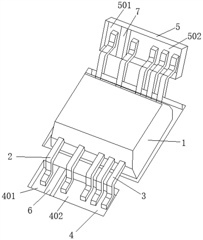
[0069] On the basis of Examples 1-2, please refer to figure 2 , also includes: the outer two ends of the package shell 1 are provided with the same connection structure 101, one end of the connection structure 101 passes through the package shell 1 and is electrically connected to the circuit board body, and the other end of the connection structure 101 respectively connected to the welding area; the connection structure 101 includes: the first control terminal 2, the first output terminal 3, the second control terminal 201, and the second output terminal 301; the welding area includes: the main board welding area 4 and the motor welding area 5.
[0070] The beneficial effect of the above technical solution is: the circuit board is arranged in the packaging shell 1, which can improve the life of the circuit board and prevent it from being damaged. An output terminal 3, which can conduct the current used for the control signal to the outside, the first control terminal 2 and ...
PUM
 Abstract
Description
Claims
Application Information


