Chip packaging method and packaging structure

A chip packaging structure and chip packaging technology, applied in electrical components, electrical solid devices, circuits, etc., can solve the problems of high cost of mold opening, low production efficiency, increased production cycle, etc., to achieve a good working environment, reduce the overall thermal The effect of resistance and good electrical channel

Pending Publication Date: 2022-02-18
新岸线(北京)科技集团有限公司
View PDF0 Cites 0 Cited by
  • Summary
  • Abstract
  • Description
  • Claims
  • Application Information

AI Technical Summary

Problems solved by technology

[0009] Due to the fixed mold, the flexibility of heat sink production is reduced; in order to meet the heat dissipation requirements of various packages, it is necessary to re-open the mold, the production cycle is increased, and the cost of mold opening is high; the surface mount heat dissipation cover is low in production efficiency and the risk of abnormality is relatively high. high

Method used


Image

  • Chip packaging method and packaging structure
  • Chip packaging method and packaging structure
  • Chip packaging method and packaging structure

Examples


Embodiment

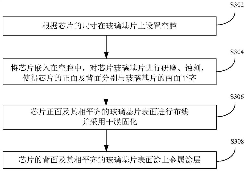
[0073] The chip packaging method provided in this embodiment has the following process steps:

[0074] Preparing the glass substrate (Glass wafer);

[0075] S101, according to the size of the chip to be packaged, perform cavity etching on the surface of the glass substrate (Glass wafer) to form a cavity, see Figure 5 ,details as follows:

[0076] On the surface of the glass substrate (Glass wafer), cover the photoresist, perform exposure and development, retain the cavity area, and then perform dry etching to complete the cavity etching and remove the surface photoresist.

[0077] S102, embedding the chip with the adhesive in the cavity. see Image 6 ,Specific steps:

[0078] Grind the chip wafer to the target thickness. Before cutting the wafer (glass substrate or chip wafer), stick an adhesive film on the back of the chip wafer. After cutting, each chip has an adhesive on the back. The chips are placed in the cavity one by one by pick up and glued and fixed.

[0079] ...


PUM


Abstract

The invention provides a chip packaging method and packaging structure, and the method comprises the steps: arranging a cavity on a glass substrate according to the size of a chip; embedding a chip into the cavity, and grinding and etching the chip and / or the glass substrate, so that the front surface and the back surface of the chip are respectively flush with the two surfaces of the glass substrate; curing the front surface of the chip and the surface of the glass substrate flush with the front surface of the chip, and wiring on the surface; and coating the back surface of the chip and the surface of the glass substrate which is flush with the back surface of the chip with metal coatings. According to the chip packaging method and the chip packaging structure provided by the invention, signal loss can be reduced, the packaging volume can be reduced, and good heat dissipation performance can be provided.

Description

technical field [0001] The invention belongs to the technical field of chip packaging, and in particular relates to a chip packaging method and a packaging structure. Background technique [0002] Common high-power and high-density chips, such as system-on-chip (SOC chip), have the advantage that multiple functions can be integrated when the substrate (wafer) is taped out. Having a higher density is faster, but has some disadvantages: [0003] like figure 1 As shown, because the SOC chip integrates multiple functions, and generally integrates multiple fixed modules, the flexibility of the chip design is reduced. For the package, it is easy to have unreasonable signal distribution on the top layer, and the substrate design is difficult. There is an increase in the substrate layer. The number of risks makes it more difficult for later packaging; [0004] The size of the SOC chip is relatively large due to the fixed space occupied by multiple IPs of the SOC core. When a lar...

Claims


Application Information

Patent Timeline
Patent Type & Authority Applications(China)
IPC IPC(8): H01L23/15H01L23/367H01L23/373H01L23/31H01L23/057H01L21/52H01L21/56
CPCH01L23/15H01L23/367H01L23/3672H01L23/3736H01L23/3121H01L23/057H01L21/52H01L21/561H01L21/568H01L2221/68327
Inventor 孙亚楠罗海峰张师群
Owner 新岸线(北京)科技集团有限公司
Why Eureka
Try Eureka