Thermal control multi-zone indium antimonide perfect wave absorber and application thereof

A technology of indium antimonide and absorber, which is applied in the field of thermally controlled multi-band indium antimonide perfect absorber, can solve the problem that the research on the number of adjustable resonance absorption peaks is rarely reported, and achieve high refraction The effect of rate sensitivity

Pending Publication Date: 2022-02-25
ZHENGZHOU UNIV
View PDF0 Cites 0 Cited by
  • Summary
  • Abstract
  • Description
  • Claims
  • Application Information

AI Technical Summary

Problems solved by technology

However, a simple design to obtain tunable numbe

Method used


Image

  • Thermal control multi-zone indium antimonide perfect wave absorber and application thereof
  • Thermal control multi-zone indium antimonide perfect wave absorber and application thereof
  • Thermal control multi-zone indium antimonide perfect wave absorber and application thereof

Examples


Embodiment 1

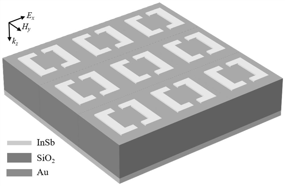
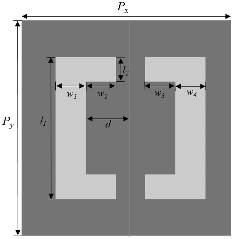
[0038] refer to Figure 1-2 , which is the structure design and top view of thermally controlled multi-band InSb perfect absorber. This structure has three layers, the upper layer is a symmetrical bracket-shaped indium antimonide array with a thickness of 0.8 μm, and the middle layer is a dielectric plate (SiO2) with a dielectric constant of 3.09 and a thickness of 15 μm. 2 ), the conductivity of the bottom layer is 4.09×10 7 S / m of metal. The structural unit parameters are: w 1 =w 2 =5μm, l 1 =15μm, l 2 = 5 μm, the space between square brackets d = 7.4 μm. The period of the structural unit along the x and y directions is P x =P y = 35 μm. Semiconductor indium antimonide is very sensitive to ambient temperature. In the terahertz range, the dielectric constant of indium antimonide is: Can be determined by the Drude model. where the high-frequency dielectric constant ε ∞ =1.68, the plasma frequency is The carrier density is

Embodiment 2

[0040] refer to Figure 1-2 , which is the structure design and top view of thermally controlled multi-band InSb perfect absorber. This structure has three layers, the upper layer is a symmetrical bracket-shaped indium antimonide array with a thickness of 0.75 μm, and the middle layer is a dielectric plate (SiO 2 ), the conductivity of the bottom layer is 4.09×10 7 S / m of metal. The structural unit parameters are: w 1 =5μm,w 2 = 3μm, l 1 = 14.9 μm, l 2 = 4.9 μm, the space between square brackets d = 5.4 μm. The period of the structural unit along the x and y directions is P x =P y = 34.5 μm. Semiconductor indium antimonide is very sensitive to ambient temperature. In the terahertz range, the dielectric constant of indium antimonide is: Can be determined by the Drude model. where the high-frequency dielectric constant ε ∞ =1.68, the plasma frequency is The carrier density is

Embodiment 3

[0042] refer to Figure 1-2 , which is the structure design and top view of thermally controlled multi-band InSb perfect absorber. This structure has three layers, the upper layer is a symmetrical bracket-shaped indium antimonide array with a thickness of 0.85 μm, and the middle layer is a dielectric plate with a dielectric constant of 3.09 and a thickness of 15.5 μm (SiO 2 ), the conductivity of the bottom layer is 4.09×10 7 S / m of metal. The structural unit parameters are: w 1 =5μm,w 2 = 3μm, l 1 = 15.1 μm, l 2 = 5.1 μm, d = 7.4 μm. The period of the structural unit along the x and y directions is P x =P y = 35.5 μm. Semiconductor indium antimonide is very sensitive to ambient temperature. In the terahertz range, the dielectric constant of indium antimonide is: Can be determined by the Drude model. where the high-frequency dielectric constant ε ∞ =1.68, the plasma frequency is The carrier density is


PUM

PropertyMeasurementUnit
Thicknessaaaaaaaaaa
Thicknessaaaaaaaaaa
Conductivityaaaaaaaaaa

Abstract

The invention discloses a thermal control multi-wave-band perfect wave absorber and application thereof. The overall structure of the thermal control multi-wave-band perfect wave absorber is composed of three layers from top to bottom, the upper layer is a square bracket indium antimonide array which is periodically arranged, the middle layer is a SiO2 medium, and the lower layer is a metal layer. At room temperature, three perfect absorption peaks can be realized at the same time by reasonably setting geometric parameters of unit structures. According to the wave absorber of the invention, the pattern structure is simple, and the perfect absorption peaks can be freely tuned from 2 to 5. The sensitive characteristic of the semiconductor indium antimonide material to the temperature is utilized, and the temperature rise can enable the whole absorption peaks to show obvious red shift. The structure of the wave absorberhas relatively high temperature sensitivity (22 GHz/K), relatively small full width at half maximum (FWHM) (0.06 THz) and relatively high refractive index sensitivity (287 GHz/RIU). The thermal control multi-band indium antimonide perfect wave absorber has a wide application prospect in the aspects of thermal control filtering, thermal biosensing, thermal imaging, detection and the like.

Description

technical field [0001] The invention belongs to the technical field of adjustable perfect wave absorbing in the terahertz band, and specifically relates to a heat-controlled multi-band indium antimonide perfect wave absorbing body and its application. Background technique [0002] A perfect absorber is a wave-absorbing device that can completely absorb incident electromagnetic waves. It is widely used in optical sensors, optical antennas, and thermal emitters. Its working mechanism is mainly based on electromagnetic resonance theory. Since the perfect absorber was proposed in 2008, it has attracted extensive research by scholars at home and abroad. So far, patterned resonators such as metal strips, split rings, closed rings, and crossed metal bars have been designed to achieve perfect wave absorption. However, these designs cannot be dynamically adjusted. [0003] InSb is a III-V binary compound semiconductor with narrow band gap, small effective mass and high electron mob...

Claims


Application Information

Patent Timeline
IPC IPC(8): H01Q17/00H01Q15/00
CPCH01Q17/00H01Q15/002H01Q15/0026
Inventor 范春珍詹影
Owner ZHENGZHOU UNIV
Why Eureka
Try Eureka