

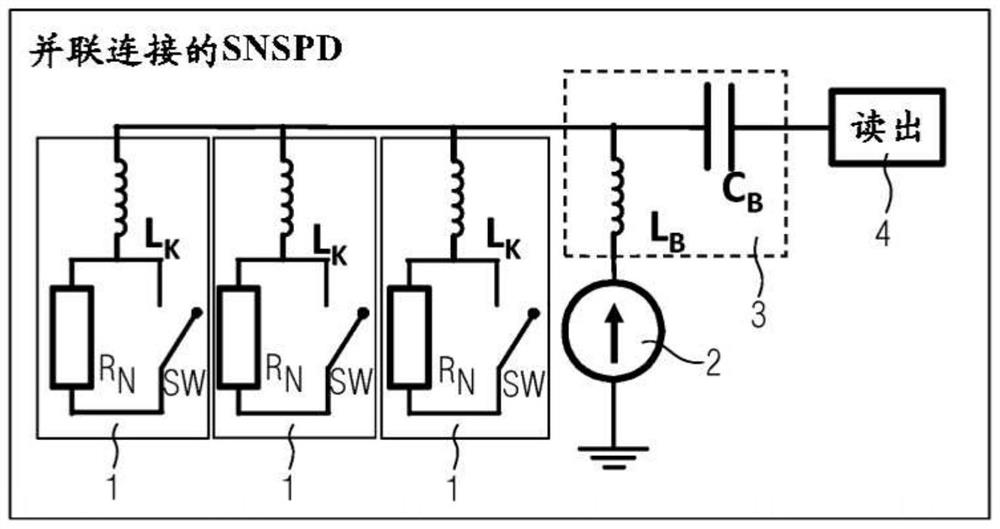
Device and system for single photon detection using plurality of superconducting detection means connected in parallel
A technology for detecting components and single photons, which is applied in the direction of photometry using electrical radiation detectors, superconductor components, and superconducting devices, and can solve problems such as equipment being unsuitable for solution.
- Summary
- Abstract
- Description
- Claims
- Application Information
AI Technical Summary
Problems solved by technology
Method used
Image

Examples
Embodiment Construction
[0021] The present invention will be described in detail below with reference to the above-mentioned drawings.
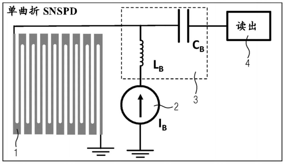
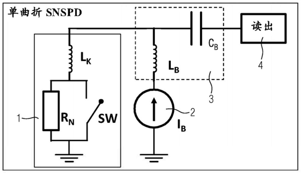
[0022] The invention relates to a device for single photon detection based on a superconducting material forming a superconducting detection component with an absorbing region for incident photons. Therefore, the rest of this description will mainly deal with the case of superconducting detection components realized by superconducting nanowires, which does not limit the scope of corresponding explanations, and the analogy extends to any type of superconducting detection components suitable for this purpose, such as , any kind of superconducting tape of suitable material and / or superconducting film or coating of suitable shape and thickness known to those skilled in the art. Therefore, and for reasons of simplification of the language used, the following description will make broad use of the terms "superconducting detection component", "superconducting nanowire" and...
PUM
 Abstract
Description
Claims
Application Information