Silicon carbide crystal growing device

A technology of crystal growth and silicon carbide, applied in the direction of crystal growth, single crystal growth, single crystal growth, etc., can solve the problems of ensuring the quality of silicon carbide crystals, the inability to guarantee the production efficiency of silicon carbide crystals, polycrystalline, etc.

Active Publication Date: 2022-03-01
江苏集芯先进材料有限公司
View PDF5 Cites 0 Cited by
  • Summary
  • Abstract
  • Description
  • Claims
  • Application Information

AI Technical Summary

Problems solved by technology

[0003] In the related art, the polycrystalline region in the silicon carbide crystal usually starts along the edge of the growth surface, and there is a large temperature gradient in the contact area between the edge of the seed crystal and the crucible and the supersaturation of the corresponding gas phase can easily lead to the generation of polycrystals in single crystals
The reason for this is that the region of the oblique growth interface from the seed growth face to the edge of the growth face is the region where enhanced "step bunching" occurs, thus leading to polytype transitions
Especially in the process of simultaneous growth of multiple sets of seed crystals, the crystal growth regulation of the contact part between the seed crystal and the edge of the seed crystal is unstable, and tends to undergo polymorphic transformation, which makes it impossible to ensure the production efficiency of silicon carbide crystals while ensuring the production efficiency of silicon carbide crystals. the quality of

Method used


Image

  • Silicon carbide crystal growing device
  • Silicon carbide crystal growing device
  • Silicon carbide crystal growing device

Examples


Embodiment Construction

[0032] Embodiments of the present invention are described in detail below, examples of which are shown in the drawings, wherein the same or similar reference numerals designate the same or similar elements or elements having the same or similar functions throughout. The embodiments described below by referring to the figures are exemplary only for explaining the present invention and should not be construed as limiting the present invention.

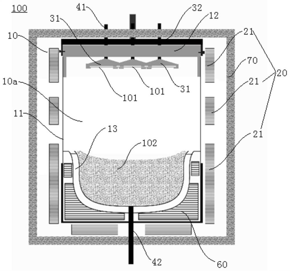
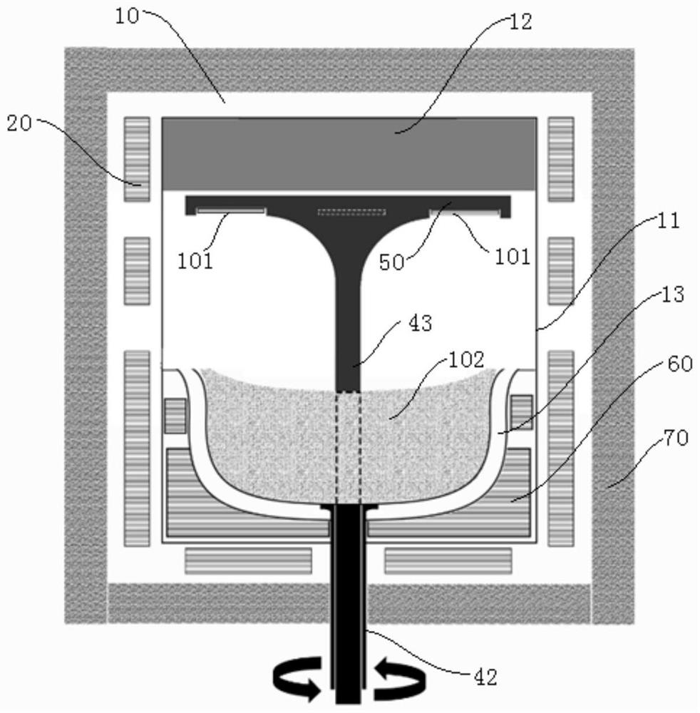
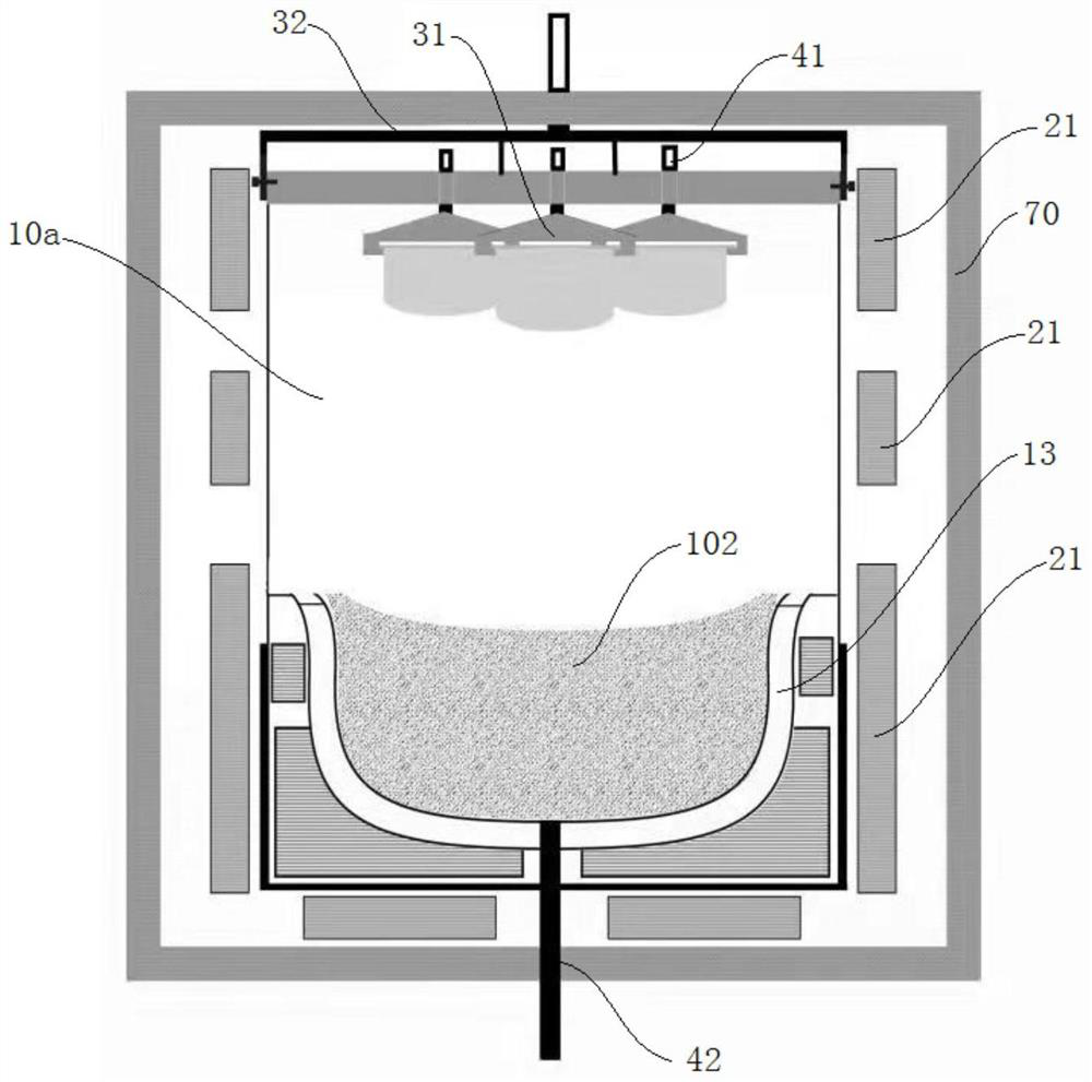
[0033] Refer below Figure 1-Figure 8 A silicon carbide crystal growth apparatus 100 according to an embodiment of the present invention is described.

[0034] The silicon carbide crystal growth device 100 according to the embodiment of the present invention includes: a furnace body, a crucible, a clamping assembly and a rotation driving assembly.

[0035] like figure 1 and figure 2 As shown, the furnace body includes a heating device 20, a reaction chamber 10a and a crucible cover 12, the heating device 20 is used to heat the reacti...


PUM


Abstract

The invention discloses a silicon carbide crystal growing device, which comprises a furnace body, a silicon carbide crystal growing device and a silicon carbide crystal growing device, the heating device is used for heating the reaction cavity; the clamping assembly comprises a plurality of seed crystal clamping parts, and the seed crystal clamping parts are arranged in the reaction cavity and are used for clamping seed crystals; the rotation driving assembly comprises a plurality of first rotation driving parts, the first rotation driving parts are connected with the seed crystal clamping part through first connecting pieces, and each first rotation driving part can independently drive the seed crystal clamping part to rotate around the central axis of the seed crystal clamped by the first rotation driving part; and the rotation directions of the seed crystals (101) are the same, so that the flowing directions of gas close to two adjacent seed crystals are opposite. Therefore, the edge temperature of the growth crystal can be homogenized, a stable SixCy steam substance mass diffusion flux is established between the silicon carbide powder and the surface of the seed crystal, and the crystal quality is improved by adjusting the crystal growth mode and inhibiting the formation of polycrystalline at the edge of the growth crystal.

Description

technical field [0001] The invention relates to the technical field of semiconductor material preparation, in particular to a silicon carbide crystal growth device. Background technique [0002] At present, in the process of growing silicon carbide single crystal, it is found that the formation of polytype switches at the edge is closely related to the stacking faults defects during the initial growth of the seed crystal surface. In general, lower stacking fault energy is the physical reason for polycrystalline generation in silicon carbide crystals. Thus, the polymorphism of SiC during high-temperature PVT growth is related to unstable growth conditions. [0003] In the related art, the polycrystalline region in the silicon carbide crystal usually starts along the edge of the growth surface. In the contact area between the edge of the seed crystal and the crucible, there is a large temperature gradient and the supersaturation of the corresponding gas phase is easy to cause...

Claims


Application Information

Patent Timeline
Patent Type & Authority Applications(China)
IPC IPC(8): C30B29/36C30B23/00
CPCC30B29/36C30B23/00
Inventor 李远田陈俊宏
Owner 江苏集芯先进材料有限公司
Why Eureka
Try Eureka