Method for improving Nor Flash polycrystalline silicon etching and dielectric layer filling process window

A process window, polysilicon layer technology, applied in electrical components, electrical solid devices, circuits, etc., can solve the problems of insufficient filling capacity of the dielectric layer, incomplete etching, easy formation of voids, etc., to avoid polysilicon etching residues, expansion, etc. The effect of etching the process window and enlarging the process window

Pending Publication Date: 2022-03-04
SHANGHAI HUALI MICROELECTRONICS CORP
View PDF0 Cites 0 Cited by
  • Summary
  • Abstract
  • Description
  • Claims
  • Application Information

AI Technical Summary

Problems solved by technology

[0007] The present invention is aimed at the conventional polysilicon layer etching, due to the existence of step height, deep depressions will be formed at the junction, resulting in the bottom anti-reflection layer (BARC) coating, in the depressions If the thickness is thicker, it is easy to etch incompletely when the subsequent polysilicon layer is etched, forming polysilicon residues, resulting in a small etching process window, and the filling capacity of the subsequent dielectric layer is insufficient, and it is easy to form voids, resulting in poor failure and other defects. Method for Flash polysilicon etching and dielectric layer filling process window

Method used


Image

  • Method for improving Nor Flash polycrystalline silicon etching and dielectric layer filling process window
  • Method for improving Nor Flash polycrystalline silicon etching and dielectric layer filling process window
  • Method for improving Nor Flash polycrystalline silicon etching and dielectric layer filling process window

Examples


Embodiment Construction

[0028] In order to illustrate the technical content, structural features, achieved goals and effects of the present invention in detail, the following will be described in detail in conjunction with the embodiments and accompanying drawings.

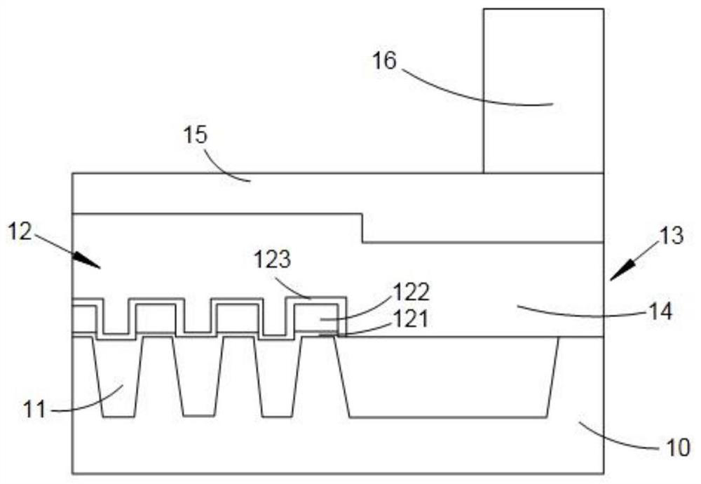
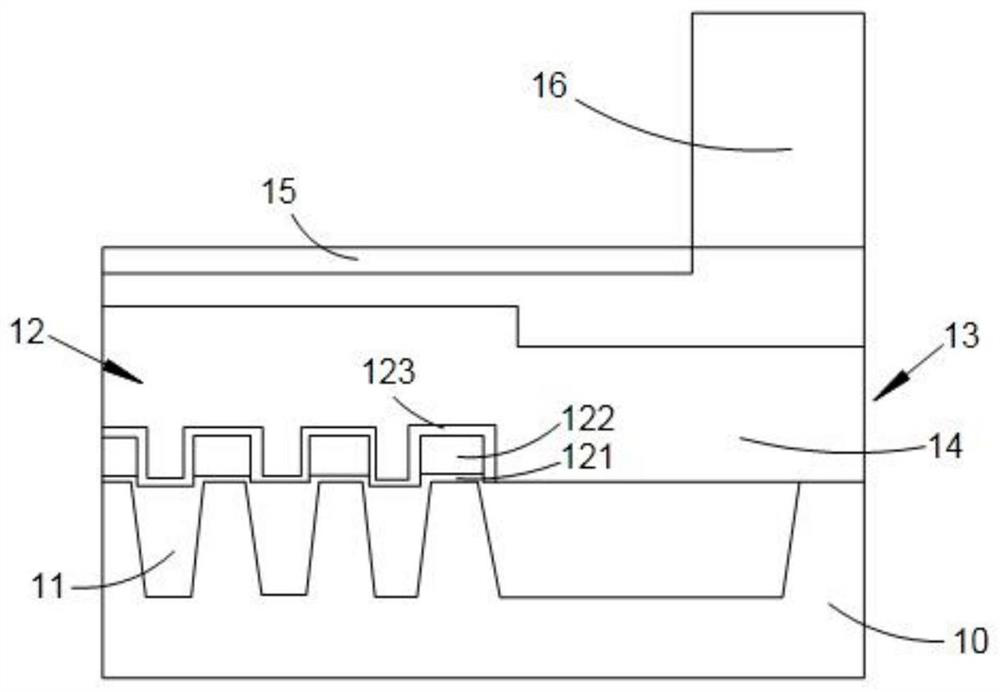
[0029] see figure 1 , figure 1 Shown is the flow chart of the method for improving the process window of Nor Flash polysilicon etching and dielectric layer filling in the present invention. In the present invention, the method for promoting the Nor Flash polysilicon etching and dielectric layer filling process window, by coating the bottom anti-reflective coating before the polysilicon layer etching, and adopting the etching-back process to reduce the area of ​​the Nor Flash storage area polysilicon layer, and reduce the height difference between the Nor Flash storage area and the peripheral area at the same time. Obviously, after using the etch-back process to reduce the thickness of the polysilicon layer in the Nor Flash storage ar...


PUM


Abstract

The invention relates to a method for lifting a Nor Flash polycrystalline silicon etching and dielectric layer filling process window, which comprises the following steps of: coating a bottom anti-reflection coating before etching a polycrystalline silicon layer, and lowering the polycrystalline silicon layer in a Nor Flash storage area by adopting an etchback process, so as to improve the Nor Flash polycrystalline silicon etching and dielectric layer filling process window, thereby improving the Nor Flash polycrystalline silicon etching and dielectric layer filling process window. And meanwhile, the height difference at the junction of the Nor Flash storage area and the peripheral area is reduced. According to the method, the bottom anti-reflection coating is coated before the polycrystalline silicon layer is etched, the polycrystalline silicon layer of the Nor Flash storage area is reduced by adopting the back-etching process, and meanwhile, the height difference of the junction of the Nor Flash storage area and the peripheral area is reduced, so that polycrystalline silicon etching residues and etching process window expansion caused by overlarge height difference during etching of the polycrystalline silicon layer can be avoided, and the yield of the Nor Flash storage area is improved. And the depth-to-width ratio between the control gates is also reduced due to the reduction of the height of the control gates (CG), and a dielectric layer filling process window is expanded.

Description

technical field [0001] The invention relates to the technical field of semiconductor manufacturing, in particular to a method for improving the process window of Nor Flash polysilicon etching and dielectric layer filling. Background technique [0002] With the continuous shrinking of the chip process node, the polysilicon (poly) gate pitch in the Nor Flash storage area is getting smaller and smaller, resulting in insufficient filling capacity of the subsequent dielectric layer, which is easy to form voids and cause failure. At the same time, because the thickness of the polysilicon layer in the storage area is thicker than that of the peripheral circuits, it is easy to leave polysilicon etching residues in the storage area. [0003] see Figure 3(a)~3(d) , Figure 3(a)~3(d) Shown is a structural schematic view of the polysilicon residue on the silicon-based substrate after the conventional polysilicon layer is etched. The Nor Flash includes a silicon-based substrate 10, a s...

Claims


Application Information

Patent Timeline
Patent Type & Authority Applications(China)
IPC IPC(8): H01L27/11531H01L27/11524H01L27/11529
CPCH10B41/35H10B41/42H10B41/41
Inventor 张俊学李东吴智勇
Owner SHANGHAI HUALI MICROELECTRONICS CORP
Why Eureka
Try Eureka