Monocrystalline silicon wafer cleaning equipment for LED (light-emitting diode) and use method thereof
A technology for single crystal silicon wafers and cleaning equipment, which is applied in the directions of cleaning methods, cleaning methods and utensils, chemical instruments and methods using liquids, etc., can solve problems such as low efficiency, poor cleaning effect, and complex structure, and achieve good results. , saving water resources, high efficiency
- Summary
- Abstract
- Description
- Claims
- Application Information
AI Technical Summary
Problems solved by technology
Method used
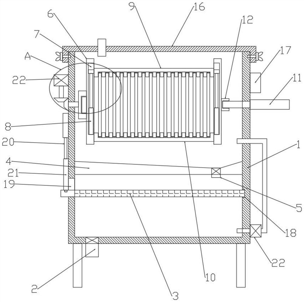
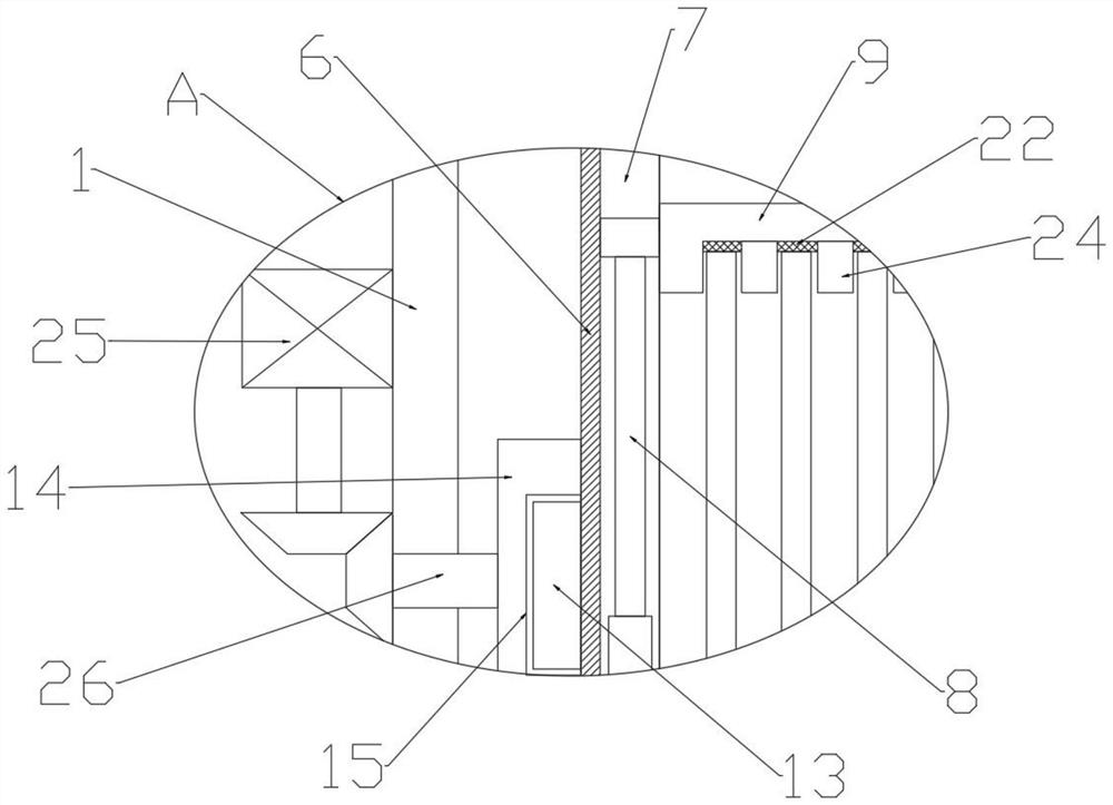
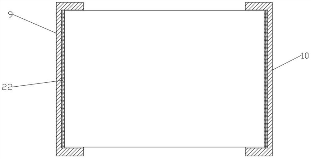
Image

Examples
Embodiment Construction
[0026] In describing the present invention, it is to be understood that the terms "central", "lateral", "upper", "lower", "left", "right", "vertical", "horizontal", "top", The orientation or positional relationship indicated by "bottom", "inner", "outer", etc. is based on the orientation or positional relationship shown in the drawings, and is only for the convenience of describing the present invention and simplifying the description, rather than indicating or implying the referred device Or elements must have a certain orientation, be constructed and operate in a certain orientation, and thus should not be construed as limiting the invention. In addition, the terms "first" and "second" are used for descriptive purposes only, and cannot be interpreted as indicating or implying relative importance or implicitly specifying the quantity of indicated technical features. Thus, a feature defined as "first" and "second" may explicitly or implicitly include one or more of these featu...
PUM
 Abstract
Description
Claims
Application Information
 - R&D
- Intellectual Property
- Life Sciences
- Materials
- Tech Scout
- Unparalleled Data Quality
- Higher Quality Content
- 60% Fewer Hallucinations
Browse by: Latest US Patents, China's latest patents, Technical Efficacy Thesaurus, Application Domain, Technology Topic, Popular Technical Reports.
© 2025 PatSnap. All rights reserved.Legal|Privacy policy|Modern Slavery Act Transparency Statement|Sitemap|About US| Contact US: help@patsnap.com