
A kind of ultraviolet lamp bead encapsulation structure and preparation method thereof

A technology of packaging structure and ultraviolet lamp, which is applied in the direction of semiconductor/solid-state device components, semiconductor devices, electrical components, etc., can solve the problems of light absorption or poor air tightness, poor antistatic ability, low optical packaging efficiency, etc., and achieve modification Improve light shape, heat dissipation effect, and improve packaging efficiency

Active Publication Date: 2022-05-31
元旭半导体科技(无锡)有限公司
View PDF13 Cites 0 Cited by
  • Summary
  • Abstract
  • Description
  • Claims
  • Application Information

AI Technical Summary

Problems solved by technology

[0005] Specifically, the technical problem to be solved by the present invention is to provide a UV lamp bead packaging structure and its preparation method to solve the problems of light absorption or poor airtightness and low light packaging efficiency in the current UVC packaging structure. , and the technical problems of poor antistatic ability and no overvoltage protection

Method used


Image

  • A kind of ultraviolet lamp bead encapsulation structure and preparation method thereof
  • A kind of ultraviolet lamp bead encapsulation structure and preparation method thereof
  • A kind of ultraviolet lamp bead encapsulation structure and preparation method thereof

Examples


Embodiment 1

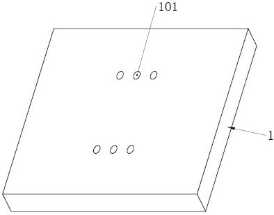
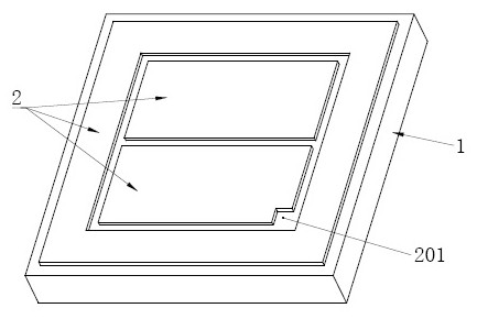
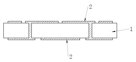
[0065] As shown in FIG. 1 to FIG. 15, the present embodiment provides an ultraviolet lamp bead packaging structure, including a substrate 1, a substrate

[0067] In this embodiment, the first metal layer 2 and the second metal layer 3 are both Ni layers, Cu layers, Ni layers, and Au layers.

[0068] In this embodiment, the two ends of the substrate 1 are respectively provided with through holes 101, the first metal layer 2, the second metal layer 3

[0070] In the present embodiment, taking the specification as a substrate with a length of 3.8mm, a width of 3.8mm and a thickness of 0.5mm as an example, the diameter of the through hole is 60 mm

[0072] In this embodiment, the P electrode region of the first metal layer 2 on the package surface of the substrate 1 is provided with an electrode identification gap 201,

[0080] S1, a substrate 1 is provided, and a through hole 101 is opened on the substrate 1 to obtain a structure 1, as shown in Figure 1;

[0081] In this step, the equ...

Embodiment 2

[0101] This embodiment is the same as the UV lamp bead packaging structure in the first embodiment, the difference is that the

Embodiment 3

[0104] This embodiment is the same as the UV lamp bead packaging structure in the first embodiment, the difference is that the

[0107] In this embodiment, the glue with conductive particles is preferably conductive silver glue.


PUM

PropertyMeasurementUnit
diameteraaaaaaaaaa
thicknessaaaaaaaaaa
thicknessaaaaaaaaaa

Abstract

The invention belongs to the technical field of LED packaging, and provides an ultraviolet lamp bead packaging structure and a preparation method thereof. The ultraviolet lamp bead packaging structure includes a substrate, the packaging surface and the back of the substrate are provided with a first metal layer, and the first metal layers on both sides The electrode area of ​​the package surface is connected, and the electrode area of ​​the first metal layer of the package surface is provided with a Zener chip, the first metal layer of the package surface also has a peripheral area, and the first metal layer of each area is respectively provided with a second metal layer. layer, the height of the electrode area of ​​the second metal layer is greater than / equal to the height of its peripheral area and the Zener chip, and the electrode area of ​​the second metal layer is provided with a UVC chip; the second metal layer is sealed with quartz through its peripheral area The lens, the quartz lens covers the UVC chip and the Zener chip, and is filled with an anti-UVC filler between the UVC chip and the Zener chip. The invention greatly improves the light encapsulation efficiency and the airtightness of the lamp bead, and greatly improves the anti-static breakdown and overvoltage protection performance of the encapsulation structure.

Description

An ultraviolet lamp bead packaging structure and preparation method thereof technical field [0001] The present invention relates to the technical field of LED packaging, in particular to a UV lamp bead packaging structure and a preparation method thereof. Background technique [0002] UVC refers to short-wave ultraviolet rays, and UVC light sources are often used in various fields such as medical treatment and pharmaceuticals. Current UVC LED's The packaging methods are divided into organic packaging, semi-inorganic packaging and all-inorganic packaging; organic packaging adopts silica gel, silicone resin or epoxy resin Resin and other organic materials; all-inorganic packaging avoids the use of organic materials throughout the process, and uses methods such as laser welding, wave soldering, and resistance welding. The combination of the lens and the substrate is realized by the method; the semi-inorganic package adopts organic silicon material with inorganic materials ...

Claims


Application Information

Patent Timeline
Patent Type & Authority Patents(China)
IPC IPC(8): H01L33/48H01L33/52H01L33/58H01L33/62H01L33/64H01L23/544H01L23/60H01L25/16
CPCH01L25/167H01L33/58H01L33/52H01L33/62H01L33/483H01L33/64H01L23/60H01L23/544H01L2933/0058H01L2933/005H01L2933/0066H01L2933/0033H01L2933/0075
Inventor 邓群雄郭文平王晓宇
Owner 元旭半导体科技(无锡)有限公司
Learn More