A filter chip wafer-level packaging structure and packaging process

A wafer-level packaging and filter technology, which is applied in the manufacturing of semiconductor devices, electric solid-state devices, and semiconductor/solid-state devices, etc., and can solve the problems of insufficient structural strength of packaged chips, insufficient mechanical strength of silicon-capped wafers, and inability to reduce thickness. , to achieve the effect of improving the structural strength of the chip package, increasing the thickness of the thinning process, and reducing the process cost

Active Publication Date: 2022-05-20
深圳新声半导体有限公司
View PDF4 Cites 0 Cited by
  • Summary
  • Abstract
  • Description
  • Claims
  • Application Information

AI Technical Summary

Problems solved by technology

[0005] The invention provides a filter chip wafer-level packaging structure and packaging process, which are used to solve the problems in the prior art that the process cost is too high, the mechanical strength of the silicon cap wafer is insufficient, and the structural strength of the packaged chip is insufficient, and the thickness cannot be reduced. , the technical solution adopted is as follows:

Method used


Image

  • A filter chip wafer-level packaging structure and packaging process
  • A filter chip wafer-level packaging structure and packaging process
  • A filter chip wafer-level packaging structure and packaging process

Examples


Embodiment Construction

[0034] The preferred embodiments of the present invention will be described below with reference to the accompanying drawings. It should be understood that the preferred embodiments described herein are only used to illustrate and explain the present invention, but not to limit the present invention.

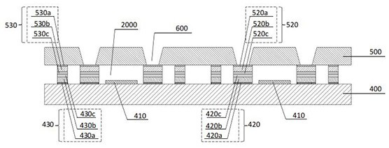
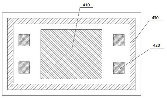
[0035] The embodiment of the present invention proposes a filter chip wafer-level packaging structure, which utilizes metal fusion bonding and eutectic bonding to realize wafer-level packaging in which a silicon cover is attached and a filter cavity is formed. When the metal bonding layer is formed on the filter wafer and the silicon cap wafer, a Cu intermediate layer is added to thicken the thickness of the entire metal stack, so that the total thickness of the metal stack on both sides reaches or exceeds 3~6 microns. Bonding is performed using the thickness of the metal stack itself to form a cavity of sufficient height without the need to etch the silicon-silicon cap substrate...


PUM

PropertyMeasurementUnit
thicknessaaaaaaaaaa
thicknessaaaaaaaaaa
distanceaaaaaaaaaa

Abstract

The invention provides a filter chip wafer-level packaging structure and packaging technology. The filter chip wafer-level packaging structure includes a filter chip wafer and a silicon lid wafer; both the filter chip wafer and the silicon lid wafer are provided with a multi-layer metal superimposed metal bonding layer; the The filter chip wafer and the silicon cap wafer are bonded and connected through the multi-layer metal stacked metal bonding layer to form a filter cavity. Wherein, the thickness of the filter cavity is not less than 2 μm. The encapsulation structure and encapsulation process can effectively reduce the process cost and improve the mechanical strength of the silicon cap wafer.

Description

technical field [0001] The invention provides a filter chip wafer-level packaging structure and packaging process, which belong to the technical field of thin film filters. Background technique [0002] Wafer-level packaging of filter chips is an indispensable link in the manufacturing process of thin-film filters. In the existing packaging structure, the electrode lead metal substrate on the filter wafer is usually composed of two layers of metal bonding layer and metal bonding layer. Metal film structure. Moreover, the groove structure is formed on the silicon cap wafer by etching to form the filter cavity, which has the following two defects: [0003] First: it is necessary to introduce an additional photolithography etching process level to form a groove cavity structure on the silicon cap 200, which is an additional process cost. [0004] Second: 200 times of etching on the silicon cap wafer into a dense groove structure, forming many convex and concave structures, re...

Claims


Application Information

Patent Timeline
Patent Type & Authority Patents(China)
IPC IPC(8): H03H3/02H03H9/10H03H9/46H01L23/31H01L21/50H01L21/56H01L21/60
CPCH03H3/02H03H9/10H03H9/46H01L23/315H01L21/50H01L21/56H01L24/83H01L2224/83
Inventor 不公告发明人
Owner 深圳新声半导体有限公司
Why Eureka
Try Eureka