HJT battery and preparation method thereof
A battery and conductive layer technology, applied in the field of solar cells, can solve the problems of poor conductivity and low power collection rate, and achieve the effects of improving conductivity and increasing electron collection rate
- Summary
- Abstract
- Description
- Claims
- Application Information
AI Technical Summary
Problems solved by technology
Method used
Image
Examples
preparation example Construction
[0052] Based on the same inventive concept, the embodiment of the present application also provides a method for preparing the above-mentioned HJT battery, including the following steps:
[0053] S1. Provide an N-type crystalline silicon wafer;
[0054] S2. Prepare intrinsic amorphous silicon layers on the front and back sides of the N-type crystalline silicon wafer;
[0055] S3, preparing a P-type amorphous silicon film layer on the surface of the intrinsic amorphous silicon layer on the front side of the N-type crystalline silicon wafer;
[0056] S4. Prepare an n-type amorphous silicon film layer on the surface of the intrinsic amorphous silicon layer on the back of the N-type crystalline silicon wafer;
[0057] S5. Prepare TCO conductive layers on the surfaces of the p-type amorphous silicon thin film layer and the n-type amorphous silicon thin film layer respectively;
[0058] S6. Prepare silver nanowire layers on the surface of the TCO conductive layer corresponding to ...
Embodiment 1
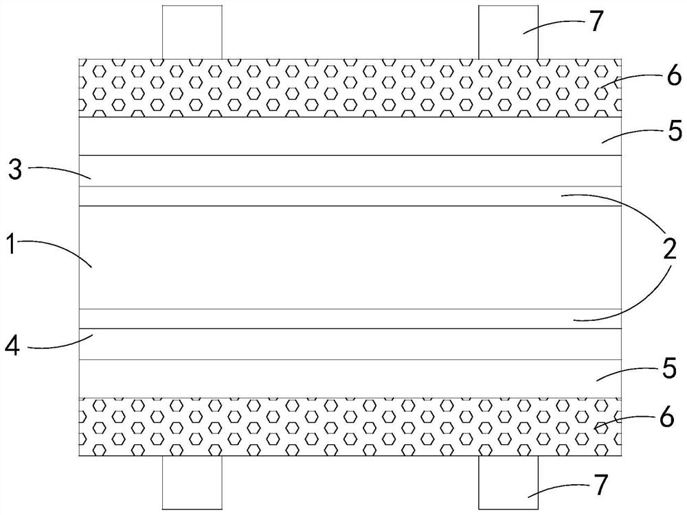
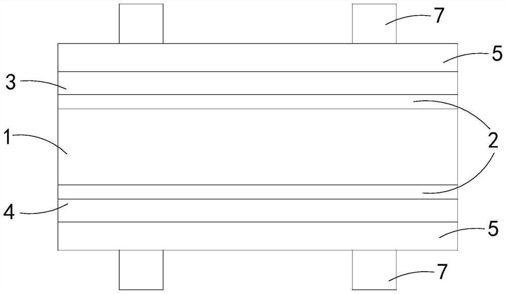
[0079] The embodiment of the present application provides a HJT battery, including:
[0080] N-type crystalline silicon wafer 1;
[0081] Intrinsic amorphous silicon layer 2, which is respectively located on the front and back of N-type crystalline silicon wafer 1;
[0082] P-type amorphous silicon thin film layer 3, which is located on the surface of intrinsic amorphous silicon layer 2 on the front side of N-type crystalline silicon wafer 1;
[0083] N-type amorphous silicon thin film layer 4, which is located on the surface of intrinsic amorphous silicon layer 2 on the back side of N-type crystalline silicon wafer 1;
[0084] TCO conductive layer 5, which is arranged on the surface of p-type amorphous silicon thin film layer 3 and n-type amorphous silicon thin film layer 4 respectively;
[0085] Silver nanowire layer 6, which is respectively located on the TCO conductive layer 5 corresponding to the p-type amorphous silicon thin film layer 3 and the corresponding TCO condu...
PUM
| Property | Measurement | Unit |
|---|---|---|
| diameter | aaaaa | aaaaa |
| thickness | aaaaa | aaaaa |
| thickness | aaaaa | aaaaa |
Abstract
Description
Claims
Application Information

