Method for controllably preparing semiconductor single-walled carbon nanotubes by combining high-throughput screening and machine learning
A single-walled carbon nanotube, semiconducting technology, applied in the field of high-throughput screening and machine learning combined with controllable preparation of semiconducting single-walled carbon nanotubes, can solve the problem of low efficiency, time-consuming semiconducting single-walled carbon nanotubes, Inaccurate and other issues, to speed up design, reduce research time and energy consumption, and standardize the effect of preparation
- Summary
- Abstract
- Description
- Claims
- Application Information
AI Technical Summary
Problems solved by technology
Method used
Image
Examples
Embodiment 1
[0045] In this example, the method for the controllable preparation of semiconducting single-walled carbon nanotubes by combining high-throughput screening and machine learning is as follows:
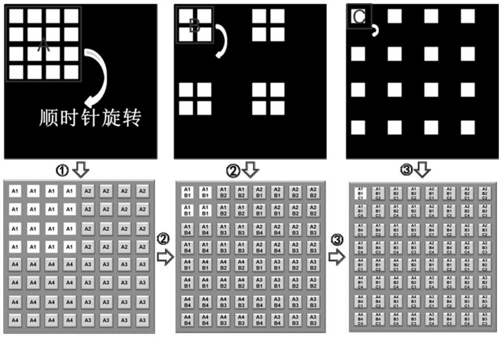
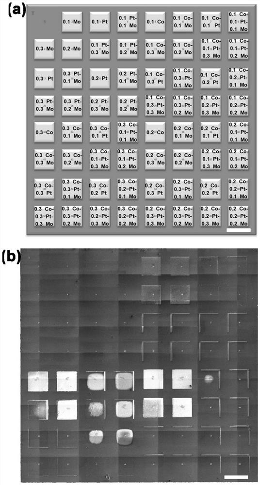
[0046] First, 64 kinds of discrete cobalt / platinum / molybdenum catalyst thin film arrays were prepared on digitally marked silicon wafers by using a combined mask to assist ion beam deposition, and the thickness range of cobalt / platinum / molybdenum catalyst thin film arrays was 0~0.9nm (excluding 0, the thickness interval is 0.1nm), the coating process see figure 1 , coating thickness and mask rotation sequence are shown in Table 1, and the cobalt / platinum / molybdenum catalyst film array prepared is shown in figure 2 (a). The growth process is as follows: first, oxidize the cobalt / platinum / molybdenum catalyst array sample at 500°C for 10 minutes in an air atmosphere, and push the sample out of the high-temperature zone; secondly, raise the temperature of the tube furnace to 850°C, After...
Embodiment 2
[0049] In this example, the method for the controllable preparation of semiconducting single-walled carbon nanotubes by combining high-throughput screening and machine learning is as follows:
[0050] First, 64 kinds of discrete cobalt / platinum / molybdenum catalyst thin film arrays were prepared on digitally marked silicon wafers by using a combined mask to assist ion beam deposition, and the thickness range of cobalt / platinum / molybdenum catalyst thin film arrays was 0~0.9nm (excluding 0, the thickness interval is 0.1nm), the coating process see figure 1 , coating thickness and mask rotation sequence are shown in Table 1, and the cobalt / platinum / molybdenum catalyst film array prepared is shown in figure 2(a). The growth process is as follows: first, oxidize the cobalt / platinum / molybdenum catalyst array sample at 500°C for 10 minutes in an air atmosphere, and push the sample out of the high-temperature zone; secondly, raise the temperature of the tube furnace to 875°C, After ...
Embodiment 3
[0053] In this example, the method for the controllable preparation of semiconducting single-walled carbon nanotubes by combining high-throughput screening and machine learning is as follows:
[0054] First, 64 kinds of discrete cobalt / platinum / molybdenum catalyst thin film arrays were prepared on digitally marked silicon wafers by using a combined mask to assist ion beam deposition, and the thickness range of cobalt / platinum / molybdenum catalyst thin film arrays was 0~0.9nm (excluding 0, the thickness interval is 0.1nm), the coating process see figure 1 , coating thickness and mask rotation sequence are shown in Table 1, and the cobalt / platinum / molybdenum catalyst film array prepared is shown in figure 2 (a). The growth process is as follows: first, oxidize the cobalt / platinum / molybdenum catalyst array sample at 500°C for 10 minutes in an air atmosphere, and push the sample out of the high-temperature zone; secondly, raise the temperature of the tube furnace to 900°C, After...
PUM
| Property | Measurement | Unit |
|---|---|---|
| thickness | aaaaa | aaaaa |
| thickness | aaaaa | aaaaa |
Abstract
Description
Claims
Application Information
 - R&D
- Intellectual Property
- Life Sciences
- Materials
- Tech Scout
- Unparalleled Data Quality
- Higher Quality Content
- 60% Fewer Hallucinations
Browse by: Latest US Patents, China's latest patents, Technical Efficacy Thesaurus, Application Domain, Technology Topic, Popular Technical Reports.
© 2025 PatSnap. All rights reserved.Legal|Privacy policy|Modern Slavery Act Transparency Statement|Sitemap|About US| Contact US: help@patsnap.com


