Method for improving durability of memory based on metal tunnel junction

A tunneling junction and memory technology, applied in static memory, read-only memory, information storage, etc., can solve the problems of difficult to achieve, poor durability, etc., and achieve the effects of improved durability, wide application range, and large adjustable parameter range

Pending Publication Date: 2022-04-05
PEKING UNIV
View PDF0 Cites 0 Cited by
  • Summary
  • Abstract
  • Description
  • Claims
  • Application Information

AI Technical Summary

Problems solved by technology

[0005] Unfortunately, at present, tunneling junction non-volatile memories are not yet able to enter mass production. One of the main reasons is that their durability is poor, and it is difficult to meet the requirements of practical applications.
However, for non-volatile memories based on tunneling junctions, when driven by voltage pulses, the reported durability is only more than 200 erasing cycles, which is still far from the lower limit of commercial indicators.

Method used


Image

  • Method for improving durability of memory based on metal tunnel junction
  • Method for improving durability of memory based on metal tunnel junction
  • Method for improving durability of memory based on metal tunnel junction

Examples


Embodiment Construction

[0044] Referring to the accompanying drawings of the present invention, the implementation process of the present invention will be described in detail below.

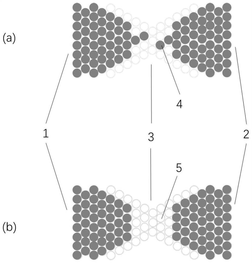
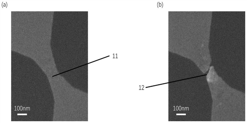
[0045] (1) Preparation of neck-containing platinum (Pt) nanoribbons: a low-resistance silicon substrate covered with a thermally oxidized silicon dioxide insulating layer is used as a device substrate. The silicon dioxide insulating layer has a thickness of 300nm. After electron beam exposure, the photoresist mask PMMA is patterned, and then electron beam evaporation is used to deposit Pt, which is soaked in acetone and stripped to obtain platinum nanoribbons with a nanometer bandwidth of about 100nm and a thickness of about 10nm ( image 3 a).

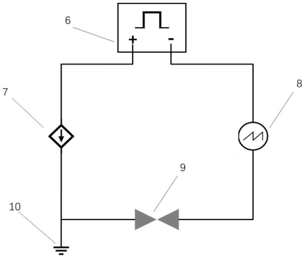
[0046] (2) Preparation of a platinum tunneling junction memory device: performing a voltage-current scan (I-V scan) on the platinum nanoribbon device above. The scanning voltage is 0-3V, the scanning speed is 0.3V / s, and a current of about 3mA can be generated in the platinu...


PUM

PropertyMeasurementUnit
thicknessaaaaaaaaaa
thicknessaaaaaaaaaa

Abstract

The invention discloses a method for improving durability of a memory based on a metal tunnel junction, and belongs to the field of nano / atomic devices. According to the principle that current-Joule heat can repair the damage of the tip of the tunneling electrode, improve the strength and increase the durability of the tunneling junction, a repair cycle is inserted in a normal erasing cycle of the metal tunneling junction memory, and the effect of current dominant migration is weakened by controlling factors such as voltage waveform, current limiting and duration of the repair cycle, so that the tunneling electrode is prevented from being damaged. And the current-Joule heat dominant migration effect is enhanced. In the repair cycle, metal atoms are fully migrated to the tip of the tunneling electrode, vacancies formed in the electric field leading migration process are filled, the strength of the tip of the tunneling electrode is enhanced, and the durability of the device is improved.

Description

technical field [0001] The invention belongs to the field of nano / atomic devices and relates to a method for improving the durability of metal tunnel junction memory. Background technique [0002] In recent years, with the rapid development of the Internet, the amount of data generated by various applications has grown rapidly. From personal consumer electronics to large-scale data centers, the requirements for large-scale data storage have made non-volatile memories, such as Flash Memory (FlashMemory), etc., It must continuously improve its own performance and integration density. At present, the semiconductor manufacturing process has advanced to 5nm and 3nm nodes, but according to the index information released by TSMC, the gate pitch and metal pitch of transistors are still at 30nm and 20nm respectively. For Metal-Oxide-Semiconductor Field-Effect Transistor (MOSFET) devices, to further improve device performance, it is possible to simultaneously improve materials, devic...

Claims


Application Information

Patent Timeline
Patent Type & Authority Applications(China)
IPC IPC(8): G11C16/26H01L45/00
Inventor 田仲政于达程任中阳田姣姣李慕禅于学敏彭沛王紫东任黎明傅云义
Owner PEKING UNIV
Why Eureka
Try Eureka