Semiconductor structure and preparation method thereof, three-dimensional memory and storage device

A semiconductor and isolation structure technology, which is applied in the field of semiconductor chips, can solve the problems of low integration of peripheral circuits of three-dimensional memory, and achieve the effects of improving cross-sectional characteristics, increasing integration, and reducing integration area

Pending Publication Date: 2022-04-05
YANGTZE MEMORY TECH CO LTD
View PDF0 Cites 0 Cited by
  • Summary
  • Abstract
  • Description
  • Claims
  • Application Information

AI Technical Summary

Problems solved by technology

[0005] Embodiments of the present disclosure provide a semiconductor structure and its preparation method, a three-dimensional memory and a storage device, aiming to solve the problem of low integration of peripheral circuits of the three-dimensional memory

Method used


Image

  • Semiconductor structure and preparation method thereof, three-dimensional memory and storage device
  • Semiconductor structure and preparation method thereof, three-dimensional memory and storage device
  • Semiconductor structure and preparation method thereof, three-dimensional memory and storage device

Examples


preparation example Construction

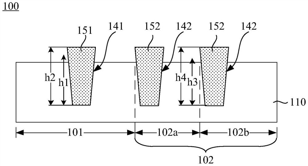
[0087] suggest a Figure 4A The manufacturing method of the semiconductor structure 100 shown includes: forming a first gate oxide layer 121 on the substrate 110, the first gate oxide layer 121 is located in the high voltage well region 101; then forming a first isolation structure 151 and a second isolation structure 152, Wherein, the first isolation structure 151 is located in the high voltage well region 101 , and the second isolation column 152 ′ is located in the low voltage well region 102 ; and then the second isolation structure 152 ′ is thinned to form the second isolation structure 152 .

[0088] However, during the fabrication of this semiconductor structure 10, as Figure 4B As shown, the gate oxide layer of the high-voltage well region 101 will be formed synchronously, which may easily cause damage to the first gate oxide layer 121 of the high-voltage well region 101 due to the hard mask integration process (such as Figure 5 shown).

[0089] Based on this, in o...


PUM

PropertyMeasurementUnit
thicknessaaaaaaaaaa
thicknessaaaaaaaaaa
thicknessaaaaaaaaaa

Abstract

The invention provides a semiconductor structure and a preparation method thereof, a three-dimensional memory and a storage device, relates to the technical field of semiconductor chips, and aims to solve the problem of low integration level of a peripheral circuit of the three-dimensional memory. The semiconductor structure can be divided into a high-voltage well region and a low-voltage well region; the semiconductor structure comprises a substrate which comprises a first groove and at least one second groove, the first groove is located in a high-voltage well region, and the second groove is located in a low-voltage well region; the first isolation structure is arranged in the first groove; the thickness of the first isolation structure is greater than the depth of the first groove; the second isolation structure is arranged in the second groove; the thickness of the second isolation structure is smaller than the depth of the second groove; the first gate oxide layer is located in the high-voltage well region; the first gate oxide layer is disposed on the surface of the substrate and exposes the first isolation structure. The semiconductor structure is applied to the three-dimensional memory so as to realize data reading and writing operation.

Description

technical field [0001] The present disclosure relates to the technical field of semiconductor chips, and in particular to a semiconductor structure and a manufacturing method thereof, a three-dimensional memory and a storage device. Background technique [0002] As the feature size of the memory cell approaches the lower limit of the process, the planar process and manufacturing technology becomes challenging and expensive, which causes the storage density of 2D or planar NAND flash memory to approach the upper limit. In order to overcome the limitations brought by 2D or planar NAND flash memory, the industry has developed a memory with a three-dimensional structure (3D NAND), which increases storage density by three-dimensionally arranging memory cells on a substrate. [0003] In the three-dimensional memory, peripheral circuits are used to perform logic operations, and to control and detect the switch states of each memory cell string to realize data storage and reading. ...

Claims


Application Information

Patent Timeline
Patent Type & Authority Applications(China)
IPC IPC(8): H01L27/11529H01L27/11556H01L27/11573H01L27/11582
Inventor 张权姚兰华子群石艳伟
Owner YANGTZE MEMORY TECH CO LTD
Why Eureka
Try Eureka