Defective product maintenance platform for semiconductor processing

A technology for defective products and semiconductors, applied in the field of repair stations for defective products, can solve problems such as increased working time and workload, reduced work efficiency, and difficult alignment, and achieves the effect of convenient repair operations and improved efficiency

Pending Publication Date: 2022-04-12
深圳市赢创智联科技有限公司
View PDF6 Cites 0 Cited by
  • Summary
  • Abstract
  • Description
  • Claims
  • Application Information

AI Technical Summary

Problems solved by technology

[0003] When packaging, the contacts on the chip are connected to the pins of the package shell through wires, and then the package cover is covered to protect the internal semiconductor chip. The existing chips are packaged in batches using packaging equipment. No, the position of the pin connection is misplaced, and it cannot be used normally after packaging, resulting in defective products. It is necessary to manually open the package, re-dock, and manually position the chip. It is not easy to align the position, and the chip is prone to occur during the welding If there is movement, there will be false soldering, and the actual pins and wires are not connected, resulting in repair failure, re-repair increases working time and workload, and reduces work efficiency

Method used


Image

  • Defective product maintenance platform for semiconductor processing
  • Defective product maintenance platform for semiconductor processing
  • Defective product maintenance platform for semiconductor processing

Examples


Embodiment Construction

[0029] The following will clearly and completely describe the technical solutions in the embodiments of the present invention with reference to the accompanying drawings in the embodiments of the present invention. Obviously, the described embodiments are only some, not all, embodiments of the present invention. Based on the embodiments of the present invention, all other embodiments obtained by persons of ordinary skill in the art without making creative efforts belong to the protection scope of the present invention.

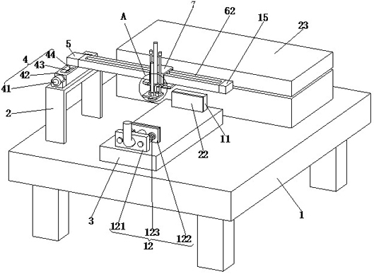
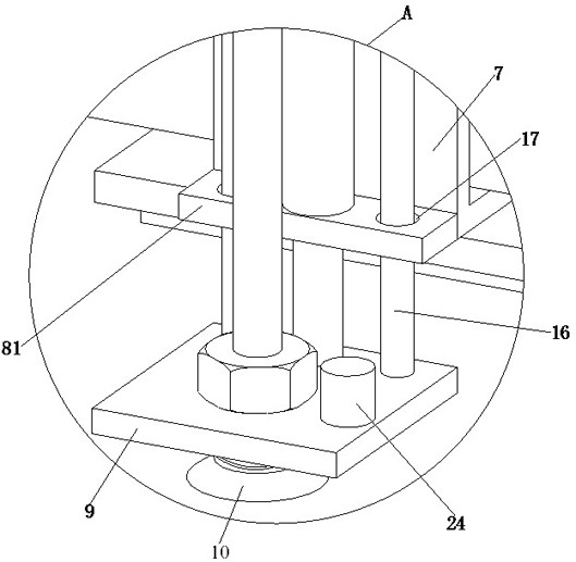
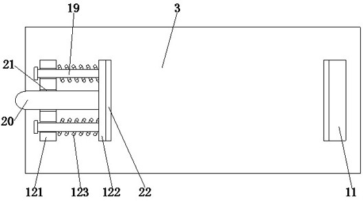
[0030] see Figure 1-8 , a repair station for defective products used in semiconductor processing, comprising: a workbench 1, a bracket 2 and a fixed platform 3 are fixedly connected to the top of the workbench 1, and a guide mechanism 4 is installed on the top of the bracket 2, and the guide mechanism 4 The top is fixedly connected with a connecting block 5, and one side of the connecting block 5 is fixedly connected with a lateral guide mechanism 6, and the ...


PUM


Abstract

The invention relates to the technical field of semiconductors, and discloses a defective product maintenance table for semiconductor processing, which comprises a working table, and the top of the working table is fixedly connected with a bracket and a fixed table. According to the defective product maintenance platform for semiconductor processing, the guide mechanism, the transverse guide mechanism and the vacuum chuck are arranged, a semiconductor chip is sucked through the vacuum chuck, a first motor of the guide mechanism is started, an output shaft of the first motor rotates to drive a first threaded rod to rotate, and the first threaded rod rotates to adjust the position of a guide block; a second motor of the transverse guide mechanism is started, an output shaft of the second motor drives a second threaded rod to rotate, the second threaded rod rotates to adjust the position of a sliding block, the sliding block drives a connecting ring to move, the connecting ring drives a lifting mechanism and a moving plate to move, and then the position of the chip can be adjusted; therefore, the position of the semiconductor chip is adjusted, and the position of the chip is convenient to adjust.

Description

technical field [0001] The invention relates to the technical field of semiconductors, in particular to a repair station for defective products used in semiconductor processing. Background technique [0002] Semiconductor refers to a material whose conductivity is between that of a conductor and an insulator at room temperature. It is used in integrated circuits, consumer electronics, communication systems, photovoltaic power generation, lighting, high-power power conversion and other fields. It is etched on semiconductor sheets. After the wiring is made into a semiconductor chip, the semiconductor chip needs to be packaged, that is, the shell for installing the semiconductor integrated circuit chip, which plays the role of placing, fixing, sealing, protecting the chip and enhancing the electrothermal performance, and also communicates the internal world of the chip with the external circuit. bridge. [0003] When packaging, the contacts on the chip are connected to the pin...

Claims


Application Information

Patent Timeline
Patent Type & Authority Applications(China)
IPC IPC(8): B23K3/08B25H1/08
Inventor 张乐单黎羚彭保生李振东王毅黄丽慧梁春晓皮进孙寿福
Owner 深圳市赢创智联科技有限公司
Why Eureka
Try Eureka