Semiconductor device forming method

A semiconductor and device technology, applied in the field of semiconductor device formation, can solve the problem of small hole etching ability, cannot meet the uniformity requirements of small-scale structure refinement process, cannot take into account the oxidation resistance of silicon nitride, etc. The uniformity of etching is high, the effect of improving CD shrinkage ability and enhancing etching selectivity

Pending Publication Date: 2022-04-12
ADVANCED MICRO FAB EQUIP INC CHINA
View PDF0 Cites 0 Cited by
  • Summary
  • Abstract
  • Description
  • Claims
  • Application Information

AI Technical Summary

Problems solved by technology

[0005] The purpose of the present invention is to solve the problem that the small-scale etching process in the prior art cannot simultaneously take into account the oxidation resistance to silicon nitride, the shrinkage ability to CD (critical dimension), and the small hole etching ability, especially the inability to Satisfies the uniformity requirements for the refinement process of small-scale structures of 3nm and below

Method used


Image

  • Semiconductor device forming method
  • Semiconductor device forming method
  • Semiconductor device forming method

Examples


Embodiment 1

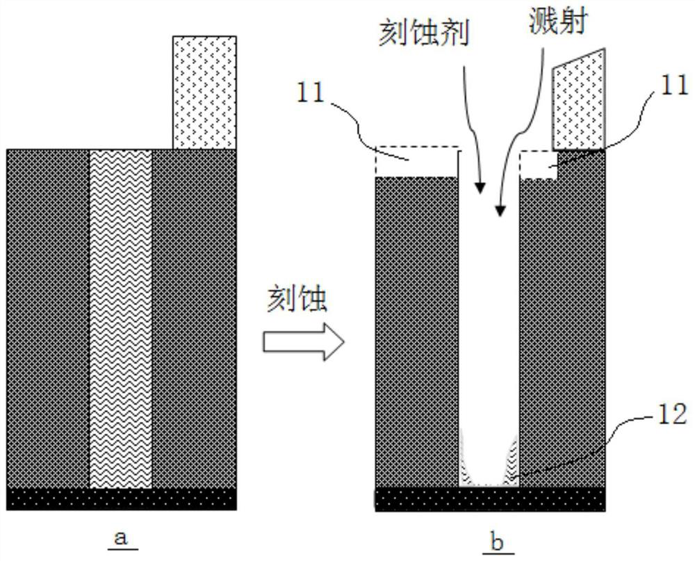
[0041] In the vacuum reaction chamber, a substrate is provided, and a dielectric layer is provided on the substrate, and the dielectric layer includes at least one opening, and a bottom anti-reflective coating is provided on the dielectric layer and in the opening. layer (BARC), a layer of photoresist (PR) is placed over the bottom anti-reflective coating around the opening.

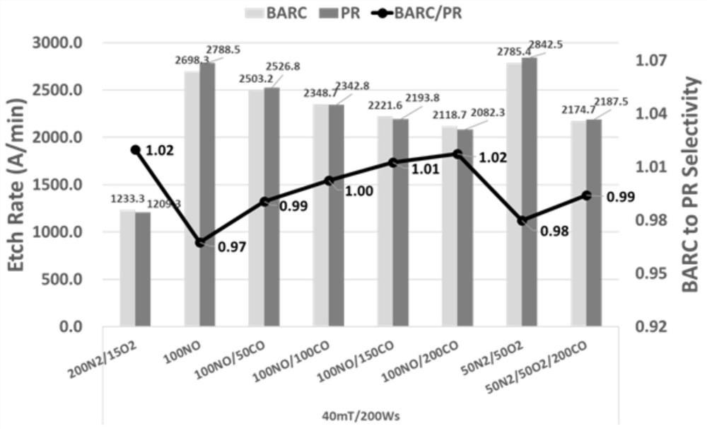
[0042] 100 units of NO were mixed with 0, 50, 100, 150 and 200 units of CO as the reaction gas to carry out the etching selectivity experiment of BARC and PR, that is, 100NO, 100NO / 50CO, 100NO / 100CO, 100NO / 150CO, 100NO / 200CO experimental group; use 200 units of N as a relatively good etching gas in the prior art 2 with 15 units of O 2 mixed as a reference group (200N 2 / 15O 2 ); and with 50N of equiatomic ratio 2 / 50O 2 , 50N 2 / 50O 2 / 200CO as a control group.

[0043] Experimental results such as image 3 shown, the reference group (200N 2 / 15O 2 ) The selection ratio of BARC and PR is 1.02...

Embodiment 2

[0048] In the vacuum reaction chamber, a substrate is provided, and a dielectric layer is provided on the substrate, and the dielectric layer includes at least one opening, and a bottom anti-reflective coating is provided on the dielectric layer and in the opening. layer (BARC), a layer of photoresist (PR) is placed over the bottom anti-reflective coating around the opening.

[0049] 100 units of NO were mixed with 0, 50, 100, 150 and 200 units of CO as the reaction gas to conduct etching rate and uniformity experiments on BARC coatings, namely, 100NO, 100NO / 50CO, 100NO / 100CO , 100NO / 150CO, 100NO / 200CO experimental groups; 50N with equiatomic ratio 2 / 50O 2 , 50N 2 / 50O 2 / 200CO as a control group.

[0050] Experimental results such as Figure 4 As shown, as the amount of CO increases, the etching rate decreases gradually, and the uniformity also decreases (NU% increases): the NU% of the experimental group increases from 2.2 to 4.2 (different processes require different N...

Embodiment 3

[0053] In the vacuum reaction chamber, a substrate is provided, and a dielectric layer is provided on the substrate, and the dielectric layer includes at least one opening, and a bottom anti-reflective coating is provided on the dielectric layer and in the opening. layer, a layer of photoresist is disposed over the bottom anti-reflective coating around the opening.

[0054] Using different reactive gases to etch the substrate, when etching the same thickness, the reference group conditions are: 200N 2 / 15O 2 Etching for 60s; the conditions of the control group were: 50N 2 / 50O 2 Etching 27s, 50N 2 / 50O 2 / 200CO etching for 35s; the experimental conditions were: 100NO etching for 28s, 100NO / 50CO etching for 30s, 100NO / 100CO etching for 32s, 100NO / 150CO etching for 34s, and 100NO / 200CO etching for 36s.

[0055] like Figure 5 As shown, after etching in the reference group, the CD size of PR is 87.28nm, and the etching rate is 1314.1A / min. A / min, the etching rate increased...


PUM

PropertyMeasurementUnit
widthaaaaaaaaaa
widthaaaaaaaaaa
sizeaaaaaaaaaa

Abstract

The invention discloses a method for forming a semiconductor device, which is carried out in a vacuum reaction cavity and comprises the following steps of: providing a substrate, arranging a dielectric substance layer on the substrate, arranging at least one opening on the substrate, arranging a bottom anti-reflection coating above the dielectric substance layer and in the opening, and arranging a photoresist layer above the bottom anti-reflection coating around the opening; reaction gas is introduced into the vacuum reaction cavity, the opening is etched, the reaction gas comprises first gas and second gas, the first gas comprises NO, the second gas comprises CO and/or CO2, and the etching rate of the reaction gas to the bottom anti-reflection coating is larger than the etching rate of the reaction gas to the photoresist layer. The NO/CO reaction gas provided by the invention can achieve the effects that the selection ratio of the BARC and the PR is equivalent to the basic condition, the etching rate of the BARC is greatly improved, the CD size of the PR is greatly reduced, the oxidation capacity of the PR to the SiN dielectric substance layer is reduced, and the subsequent wet etching wafer loss is reduced, and the etching uniformity can also meet the requirement.

Description

technical field [0001] The invention belongs to the technical field of semiconductors, and in particular relates to a method for forming a semiconductor device. Background technique [0002] The chip industry is being updated day by day, the technology nodes are improving day by day, and the requirements for craftsmanship and technology are getting higher and higher, especially at 3nm and below, the refined process is becoming more and more prominent, such as the uniformity of most processes, Regardless of thin film deposition, etching, polishing and other processes, high uniformity is required with the improvement of nano-nodes. In terms of etching, for example, the precision of the process, low damage or strong etching ability is required. [0003] At present, at 3nm and below, the etching of organic materials is facing great challenges, especially the etching of small holes (less than 15nm), which has a high aspect ratio, and the etching ability at the bottom of the smal...

Claims


Application Information

Patent Timeline
Patent Type & Authority Applications(China)
IPC IPC(8): H01L21/027H01L21/311
Inventor 赵军苏兴才
Owner ADVANCED MICRO FAB EQUIP INC CHINA
Why Eureka
Try Eureka